 | –≠–ª–µ–∫—Ç—Ä–æ–Ω–Ω—ã–π –∫–æ–º–ø–æ–Ω–µ–Ω—Ç: LF13508D | –°–∫–∞—á–∞—Ç—å:  PDF PDF  ZIP ZIP |
TL H 5668
LF13508
8-Channel
Analog
Multiplexer
LF13509
4-Channel
Differential
Analog
Multiplexer
January 1995
LF13508 8-Channel Analog Multiplexer
LF13509 4-Channel Differential Analog Multiplexer
General Description
The LF13508 is an 8-channel analog multiplexer which con-
nects the output to 1 of the 8 analog inputs depending on
the state of a 3-bit binary address An enable control allows
disconnecting the output thereby providing a package se-
lect function
This device is fabricated with National's BI-FET technology
which provides ion-implanted JFETs for the analog switch
on the same chip as the bipolar decode and switch drive
circuitry This technology makes possible low constant
``ON'' resistance with analog input voltage variations This
device does not suffer from latch-up problems or static
charge blow-out problems associated with similar CMOS
parts The digital inputs are designed to operate from both
TTL and CMOS levels while always providing a definite
break-before-make action
The LF13509 is a 4-channel differential analog multiplexer
A 2-bit binary address will connect a pair of independent
analog inputs to one of any 4 pairs of independent analog
outputs The device has all the features of the LF13508
series and should be used whenever differential analog in-
puts are required
Features
Y
JFET switches rather than CMOS
Y
No static discharge blow-out problem
Y
No SCR latch-up problems
Y
Analog signal range 11V
b
15V
Y
Constant ``ON'' resistance for analog signals between
b
11V and 11V
Y
``ON'' resistance 380 X typ
Y
Digital inputs compatible with TTL and CMOS
Y
Output enable control
Y
Break-before-make action t
OFF
e
0 2 ms t
ON
e
2 ms typ
Y
Lower leakage devices available
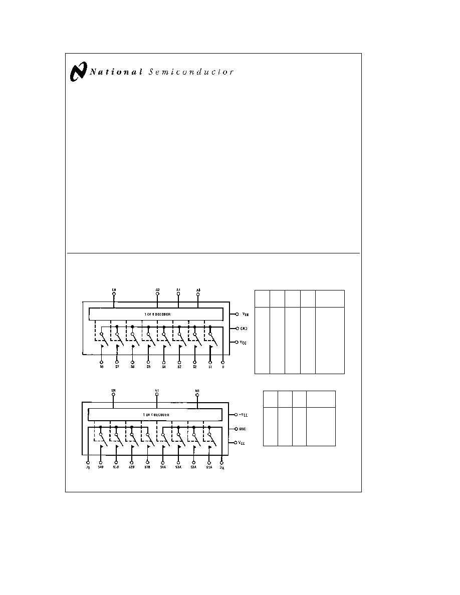
Functional Diagrams and Truth Tables
LF13508
EN
A2
A1
A0
SWITCH
ON
H
L
L
L
S1
H
L
L
H
S2
H
L
H
L
S3
H
L
H
H
S4
H
H
L
L
S5
H
H
L
H
S6
H
H
H
L
S7
H
H
H
H
S8
L
X
X
X
NONE
LF13509
EN
A1
A0
SWITCH
PAIR ON
L
X
X
None
H
L
L
S1
H
L
H
S2
H
H
L
S3
H
H
H
S4
TL H 5668 ≠ 1
C1995 National Semiconductor Corporation
RRD-B30M115 Printed in U S A

Absolute Maximum Ratings
If Military Aerospace specified devices are required
please contact the National Semiconductor Sales
Office Distributors for availability and specifications
Positive Supply
b
Negative Supply (V
CC
b
V
EE
)
36V
Positive Analog Input Voltage (Note 1)
V
CC
Negative Analog Input Voltage (Note 1)
b
V
EE
Positive Digital Input Voltage
V
CC
Negative Digital Input Voltage
b
5V
Analog Switch Current
l
I
S
l
k
10 mA
Power Dissipation (P
D
at 25 C)
(Notes 2
7)
Molded DIP (N)
P
D
500 mW
Cavity DIP (D)
P
D
900 mW
Small Outline (SO) P
D
500 mW
Maximum Junction Temperature (T
jMAX
)
100 C
Operating Temperature Range
0 C
s
T
A
s
a
70 C
Storage Temperature Range
b
65 C to
a
150 C
Lead Temperature
D Package (Soldering 10 seconds)
300 C
N Package (Soldering 10 seconds)
260 C
Surface Mount Package (SO)
Vapor Phase (60 seconds)
215 C
Infrared (15 seconds)
220 C
Electrical Characteristics
(Note 3)
LF13508
Symbol
Parameter
Conditions
LF13509
Units
Min
Typ
Max
R
ON
``ON'' Resistance
V
OUT
e
0V I
S
e
100 mA
T
A
e
25 C
380
650
X
500
850
X
D
R
ON
D
R
ON
with Analog Voltage
b
10V
s
V
OUT
s
a
10V I
S
e
100 mA
T
A
e
25 C
0 01
1
%
Swing
R
ON
Match
R
ON
Match Between Switches
V
OUT
e
0V I
S
e
100 mA
T
A
e
25 C
20
150
X
I
S(OFF)
Source Current in ``OFF''
Switch ``OFF'' V
S
e
11 V
D
e b
11
T
A
e
25 C
5
nA
Condition
(Note 4)
0 09
50
nA
I
D(OFF)
Drain Current in ``OFF''
Switch ``OFF'' V
S
e
11 V
D
e b
11
T
A
e
25 C
20
nA
Condition
(Note 4)
0 6
500
nA
I
D(ON)
Leakage Current in ``ON''
Switch ``ON'' V
D
e
11V (Note 4)
T
A
e
25 C
20
nA
Condition
1
500
nA
V
INH
Digital ``1'' Input Voltage
2 0
V
V
INL
Digital ``0'' Input Voltage
0 7
V
I
INL
Digital ``0'' Input Current
V
IN
e
0 7V
T
A
e
25 C
1 5
30
m
A
40
m
A
I
INL(EN)
Digital ``0'' Enable Current
V
EN
e
0 7V
T
A
e
25 C
1 2
30
m
A
40
m
A
t
TRAN
Switching Time of Multiplexer
(Figure 1) (Note 5)
T
A
e
25 C
1 8
m
s
t
OPEN
Break-Before-Make
(Figure 3)
T
A
e
25 C
1 6
m
s
t
ON(EN)
Enable Delay ``ON''
(Figure 2)
T
A
e
25 C
1 6
m
s
t
OFF(EN)
Enable Delay ``OFF''
(Figure 2)
T
A
e
25 C
0 2
m
s
I
SO(OFF)
``OFF'' Isolation
(Note 6)
T
A
e
25 C
b
66
dB
CT
Crosstalk
LF13509 Series (Note 6)
T
A
e
25 C
b
66
dB
C
S(OFF)
Source Capacitance (``OFF'')
Switch ``OFF'' V
OUT
e
0V
T
A
e
25 C
2 2
pF
V
S
e
0V
C
D(OFF)
Drain Capacitance (``OFF'')
Switch ``OFF'' V
OUT
e
0V
T
A
e
25 C
11 4
pF
V
S
e
0V
I
CC
Positive Supply Current
All Digital Inputs Grounded
T
A
e
25 C
7 4
12
mA
7 9
15
mA
I
EE
Negative Supply Current
All Digital Inputs Grounded
T
A
e
25 C
2 7
5
mA
2 8
6
mA
2

Electrical Characteristics
(Continued)
Note 1
If the analog input voltage exceeds this limit the input current should be limited to less than 10 mA
Note 2
The maximum power dissipation for these devices must be derated at elevated temperatures and is dictated by T
jMAX
i
jA
and the ambient temperature
T
A
The maximum available power dissipation at any temperature is P
D
e
(T
jMAX
b
T
A
) i
jA
or the 25 C P
DMAX
whichever is less
Note 3
These specifications apply for V
S
e g
15V and over the absolute maximum operating temperature range (T
L
s
T
A
s
T
H
) unless otherwise noted
Note 4
Conditions applied to leakage tests insure worse case leakages Exceeding 11V on the analog input may cause an ``OFF'' channel to turn ``ON''
Note 5
Lots are sample tested to this parameter The measurement conditions of
Figure 1 insure worse case transition time
Note 6
``OFF'' isolation is measured with all switches ``OFF'' and driving a source Crosstalk is measured with a pair of switches ``ON'' driving channel A and
measuring channel B R
L
e
200 C
L
e
7 pF V
S
e
3 Vrms f
e
500 kHz
Note 7
Thermal Resistance i
jA
(Junction to Ambient)
Molded DIP (N)
150 C W
Cavity DIP (D)
100 C W
Connection Diagrams
LF13508
Dual-In-Line (N or D) or Small Outline (SO) Packages
LF13509
Dual-In-Line (N or D) or Small Outline (SO) Packages
TL H 5668 ≠ 2
Order Number LF13508D
See NS Package Number D16C
Order Number LF13508M
See NS Package Number M16A
Order Number LF13508N
See NS Package Number N16A
Order Number LF13509D
See NS Package Number D16C
Order Number LF13509M
See NS Package Number M16A
Order Number LF13509N
See NS Package Number N16A
AC Test Circuits and Switching Time Waveforms
TL H 5668 ≠ 3
FIGURE 1 Transition Time
3
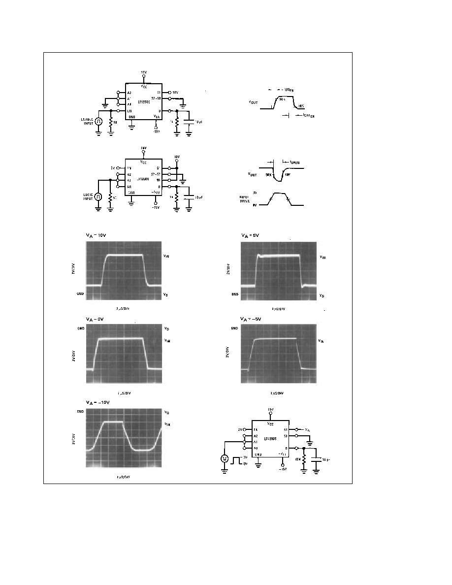
AC Test Circuit and Switching Time Waveforms
(Continued)
FIGURE 2 Enable Times
TL H 5668 ≠ 4
FIGURE 3 Break-Before-Make
Transition Times and Transients
TL H 5668 ≠ 5
TL H 5668 ≠ 6
TL H 5668 ≠ 7
TL H 5668 ≠ 8
TL H 5668 ≠ 9
Test Circuit
TL H 5668 ≠ 10
4

Typical Performance Characteristics
``ON'' Resistance
``ON'' Resistance
``ON'' Resistance
Switch Leakage
Currents
Switch Leakage
Currents
Switch Leakage
Currents
Switching Times
(Figures 1 and 3)
Enable Delay Times
(Figure 2)
``OFF'' Isolation and
Crosstalk
Bias Currents
Supply Currents
Switch Capacitances
TL H 5668 ≠ 11
5