
TL K 5558
LH0101
Power
Operational
Amplifier
February 1995
LH0101 Power Operational Amplifier
General Description
The LH0101 is a wideband power operational amplifier fea-
turing FET inputs internal compensation virtually no cross-
over distortion and rapid settling time These features make
the LH0101 an ideal choice for DC or AC servo amplifiers
deflection yoke drives programmable power supplies and
disk head positioner amplifiers The LH0101 is packaged in
an 8 pin TO-3 hermetic package rated at 60 watts with a
suitable heat sink
Features
Y
5 Amp peak 2 Amp continuous output current
Y
300 kHz power bandwidth
Y
850 mW standby power (
g
15V supplies)
Y
300 pA input bias current
Y
10 V ms slew rate
Y
Virtually no crossover distortion
Y
2 ms settling time to 0 01%
Y
5 MHz gain bandwidth
Schematic and Connection Diagrams
TL K 5558 ≠ 1
TL K 5558 ≠ 2
Top View
Order Numbers LH0101K
LH0101K-MIL LH0101CK
LH0101AK
LH0101AK-MIL or LH0101ACK
See NS Package Number K08A
Note Electrically connected internally no
connection should be made to pin
C1995 National Semiconductor Corporation
RRD-B30M115 Printed in U S A
Absolute Maximum Ratings
If Military Aerospace specified devices are required
please contact the National Semiconductor Sales
Office Distributors for availability and specifications
(Note 5)
Supply Voltage V
S
g
22V
Power Dissipation at T
A
e
25 C P
D
5W
Derate linearly at 25 C W to zero at 150 C
Power Dissipation at T
C
e
25 C
62W
Derate linearly at 2 C W to zero at 150 C
Differential Input Voltage V
IN
g
40V but
k g
V
S
Input Voltage Range V
CM
g
20V but
k g
V
S
Thermal Resistance
See Typical Performance Characteristics
Peak Output Current (50 ms pulse) I
O(PK)
5A
Output Short Circuit Duration
(within rated power dissipation
R
SC
e
0 35X T
A
e
25 C)
Continuous
Operating Temperature Range T
A
LH0101AC LH0101C
b
25 C to
a
85 C
LH0101A LH0101
b
55 C to
a
125 C
Storage Temperature Range T
STG
b
65 C to
a
150 C
Maximum Junction Temperature T
J
150 C
Lead Temperature (Soldering
k
10 sec )
260 C
ESD rating to be determined
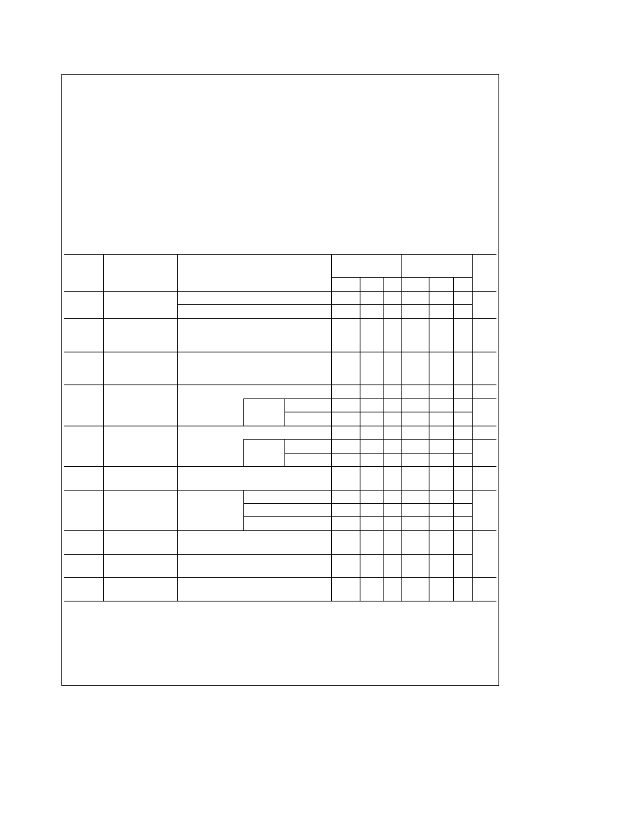
DC Electrical Characteristics
(Note 1) V
S
e
g
15V T
A
e
25 C unless otherwise noted
LH0101AC
LH0101C
Symbol
Parameter
Conditions
LH0101A
LH0101
Units
Min
Typ
Max
Min
Typ
Max
V
OS
Input Offset Voltage
1
3
5
10
mV
T
MIN
s
T
A
s
T
MAX
7
15
D
V
OS
D
P
D
Change in
(Note 2)
Input Offset Voltage
150
300
m
V W
with Dissipated Power
D
V
OS
D
T
Change in
V
CM
e
0
Input Offset Voltage
10
10
m
V C
with Temperature
I
B
Input Bias Current
300
1000
pA
T
A
s
T
MAX
LH0101C AC
60
60
nA
LH0101 A
300
1000
I
OS
Input Offset Current
75
250
pA
T
A
s
T
MAX
LH0101C AC
15
15
nA
LH0101 A
75
250
A
VOL
Large Signal
V
O
e
g
10V R
L
e
10X
50
200
50
200
V mV
Voltage Gain
V
O
Output Voltage Swing R
SC
e
0
R
L
e
100X
g
12
g
12 5
g
12
g
12 5
A
V
e a
1
R
L
e
10X
g
11 25
g
11 6
g
11 25
g
11 6
V
Note 3
R
L
e
5X
g
10 5
g
11
g
10 5
g
11
CMRR
Common Mode
D
V
IN
e
g
10V
85
100
85
100
Rejection Ratio
dB
PSRR
Power Supply
D
V
S
e
g
5V to
g
15V
85
100
85
100
Rejection Ratio
I
S
Quiescent Supply
28
35
28
35
mA
Current
2

AC Electrical Characteristics
(Note 1) V
S
e
g
15V T
A
e
25 C
LH0101
LH0101C
Symbol
Parameter
Conditions
LH0101A
LH0101AC
Units
Min
Typ
Max
Min
Typ
Max
e
n
Equivalent Input
f
e
1 kHz
25
25
nV
0
Hz
Noise Voltage
C
IN
Input Capacitance
f
e
1 MHz
3 0
3 0
pF
Power Bandwidth
b
3 dB
300
300
kHz
SR
Slew Rate
7 5
10
10
V ms
R
L
e
10X
(Note 4)
t
r
t
f
Small Signal Rise or
A
V
e a
1
200
200
ns
Fall Time
Small Signal Overshoot
10
10
%
GBW
Gain-Bandwidth Product
4 0
5 0
5 0
MHz
R
L
e
%
(Note 4)
t
s
Large Signal Settling
2 0
2 0
m
s
Time to 0 01%
THD
Total Harmonic Distortion
P
o
e
10W f
e
1 kHz
0 008
0 008
%
R
L
e
10X
Note 1
Specification is at T
A
e
25 C Actual values at operating temperature may differ from the T
A
e
25 C value When supply voltages are
g
15V quiescent
operating junction temperature will rise approximately 20 C without heat sinking Accordingly V
OS
may change 0 5 mV and I
B
and I
OS
will change significantly
during warm-ups Refer to the I
B
vs temperature and power dissipation graphs for expected values Power supply voltage is
g
15V Temperature tests are made
only at extremes
Note 2
Change in offset voltage with dissipated power is due entirely to average device temperature rise and not to differential thermal feedback effects Test is
performed without any heat sink
Note 3
At light loads the output swing may be limited by the second stage rather than the output stage See the application section under ``Output swing
enhancement'' for hints on how to obtain extended operation
Note 4
These parameters are sample tested to 10% LTPD
Note 5
Refer to RETS0101AK for the LH0101AK military specifications and RETS0101K for the LH0101K military specifications
3

Typical Performance Characteristics
Maximum Power Dissipation
Safe Operating Area
Current
Quiescent Power Supply
Input Bias Current
Warm-up
Input Bias Current after
Voltage Range
Input Common-Mode
Response (open loop)
Small Signal Frequency
vs Frequency
Output Voltage Swing
Ratio vs Frequency
Common-Mode Rejection
Ratio vs Frequency
Power Supply Rejection
Settling Time
Distortion vs Frequency
Total Harmonic
TL K 5558 ≠ 3
4

Typical Performance Characteristics
(Continued)
Distortion vs Gain
Total Harmonic
Equivalent Input Noise Voltage
with Swing Enhancement
Output Voltage Swing
Load Resistance
Output Voltage Swing vs
Open-Loop Output Resistance
Resistance vs Frequency
Open-Loop Output
vs R
SC
Short Circuit Current
TL K 5558 ≠ 4
Small Signal Pulse Response (No Load)
TL K 5558 ≠ 5
Large Signal Pulse Response (R
L
e
10X)
TL K 5558 ≠ 6
5