 | –≠–ª–µ–∫—Ç—Ä–æ–Ω–Ω—ã–π –∫–æ–º–ø–æ–Ω–µ–Ω—Ç: LH1605CK | –°–∫–∞—á–∞—Ç—å:  PDF PDF  ZIP ZIP |
TL K 10114
LH1605LH1605C
5
Amp
High
Efficiency
Switching
Regulator
February 1995
LH1605 LH1605C
5 Amp High Efficiency Switching Regulator
General Description
The LH1605 is a hybrid switching regulator with high output
current capabilities It incorporates a temperature-compen-
sated voltage reference a duty cycle modulator with the
oscillator frequency programmable error amplifier high cur-
rent-high voltage output switch and a power diode The
LH1605 can supply up to 5A of output current over a wide
range of regulated output voltage
Features
Y
Step down switching regulator
Y
Output adjustable from 3 0V to 30V
Y
5A output current
Y
High efficiency
Y
Frequency adjustable to 100 kHz
Y
Standard 8-pin TO-3 package
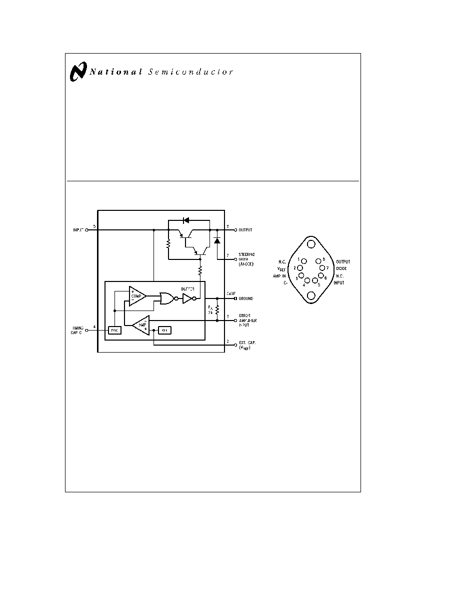
Block and Connection Diagrams
TL K 10114 ≠ 1
Case is Ground
TL K 10114 ≠ 2
Top View
Order Number LH1605K or
LH1605CK
See NS Package Number K08A
C1995 National Semiconductor Corporation
RRD-B30M115 Printed in U S A
Absolute Maximum Ratings
If Military Aerospace specified devices are required
please contact the National Semiconductor Sales
Office Distributors for availability and specifications
Input Voltage (V
IN
)
35V max
Output Current (I
O
)
6A
Operating Temperature (T
J
)
150 C
Internal Power Dissipation (P
D
) (Note 1)
20W
Operating Temperature (T
A
)
LH1605C
b
25 C to
a
85 C
LH1605
b
55 C to
a
125 C
Storage Temperature Range (T
STG
)
b
65 C to
a
150 C
Duty Cycle (D C )
20% to 80%
Steering Diode Reverse Voltage
(V
R
) (V
8 ≠ 7
)
60V
Steering Diode Forward Current
(I
D
) (I
7 ≠ 8
)
6A
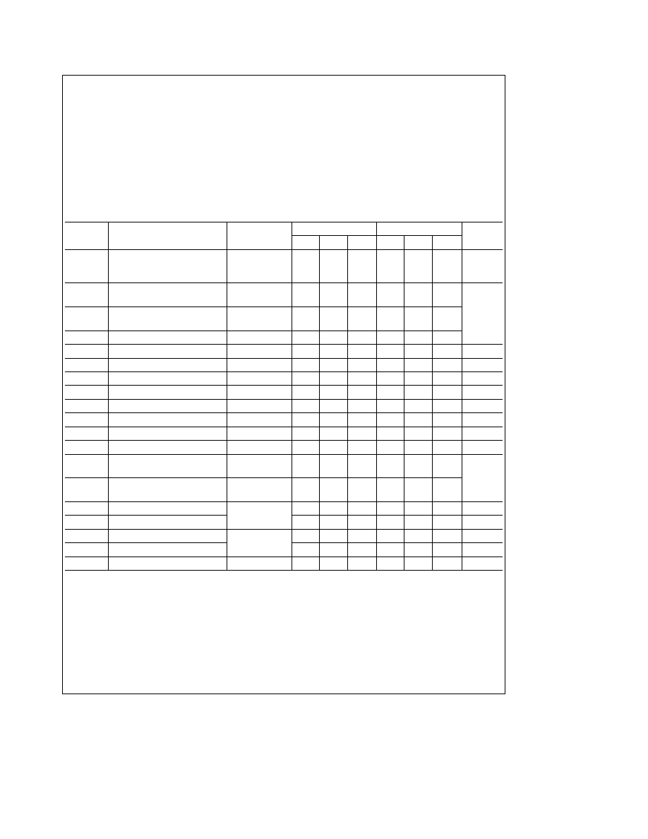
Electrical Characteristics
T
C
e
25 C V
IN
e
15V V
OUT
e
10V unless otherwise specified
Symbol
Characteristics
Conditions
LH1605
LH1605C
Units
Min
Typ
Max
Min
Typ
Max
V
OUT
Output Voltage Range
V
IN
t
V
O
a
5V
3 0
30
3 0
30
I
O
e
2A
(Note 2)
V
S
Switch Saturation Voltage
I
C
e
5 0A
1 6
2 0
1 6
2 0
I
C
e
2 0A
1 0
1 2
1 0
1 2
V
F
Steering Diode On Voltage
I
D
e
5 0A
1 2
2 8
1 2
2 8
V
I
D
e
2 0A
1 0
2 0
1 0
2 0
V
IN
Supply Voltage Range
10
35
10
35
I
R
Steering Diode Reverse Current
V
R
e
25V
0 1
5 0
0 1
5 0
m
A
I
Q
Quiescent Current
I
OUT
e
0 2A
20
20
mA
V
2
Voltage on Pin 2
2 5
2 5
V
D
V
2
D
T
V
2
Temperature Coeff
100
100
ppm C
V
4
Voltage Swing
Pin 4
3 0
3 0
V
I
4
Charging Current
Pin 4
70
70
m
A
R
A
Resistance Pin 3 to GND
2 0
2 0
kX
D
R
A
D
T
Resistance Temp Coeff
75
75
ppm C
t
r
Voltage Rise Time
I
OUT
e
2 0A
350
350
I
OUT
e
5 0A
500
500
ns
t
f
Voltage Fall Time
I
OUT
e
2 0A
300
300
I
OUT
e
5 0A
400
400
t
s
Storage Time
I
OUT
e
5 0A
1 5
1 5
m
s
t
d
Delay Time
100
100
ns
P
D
Power Dissipation
V
OUT
e
10V
16
16
W
h
Efficiency
I
OUT
e
5 0A
75
75
%
i
JC
Thermal Resistance (Note 1)
5 0
5 0
C W
Note 1 i
JA
is typically 30 C W for natural convection cooling
Note 2
V
OUT
refers to the output voltage range of switching supply after the output LC filter as shown in the Typical Application circuit
2

TL K 10114 ≠ 3
Minimum V
IN
b
V
OUT
e
5V for Proper Operation
R
S
e
2
c
10
3
(V
OUT
b
2 5)
2 5
V
IN
e
10
b
18V
V
OUT
e
5V
I
OUT
e
3A (Max)
I
OUT
e
1A (Min)
h j
70%
Load Reg
e
50 mV
Line Reg
e
10 mV
Ripple
e
20 mV
Power Derating Curve
TL K 10114 ≠ 4
Frequency vs Timing
Capacitance
TL K 10114 ≠ 5
Design Equations
Efficiency (h)
e
P
OUT
c
100
P
IN
Transistor DC Losses (P
T
)
e
I
OUT
c
V
S
t
ON
t
ON
a
t
OFF
J
Diode DC Losses (P
D
)
e
I
OUT
c
V
F
t
OFF
t
ON
a
t
OFF
J
Drive Circuit Losses (D
L
)
e
V
IN
2
300
c
t
ON
t
ON
a
t
OFF
Switching Losses Transistor (P
S
)
e
V
IN
c
I
OUT
c
t
r
a
t
f
2(t
ON
a
t
OFF
Transistor Duty Cycle
e
t
ON
t
ON
a
t
OFF
e
V
OUT
V
IN
Diode Duty Cycle
e
t
OFF
t
ON
a
t
OFF
e
1
b
V
OUT
V
IN
Power Inductor (P
L
)
e
I
OUT
2 c
R
L
(Winding Resistance)
Efficiency (h)
e
V
OUT
I
OUT
V
OUT
I
OUT
a
P
T
a
P
D
a
D
L
a
P
S
a
P
L
c
100%
3

LH1605LH1605C
5
Amp
High
Efficiency
Switching
Regulator
Physical Dimensions
inches (millimeters)
Lit
106377
8-Lead TO-3 Metal Can Package (K)
NS Package Number K08A
LIFE SUPPORT POLICY
NATIONAL'S PRODUCTS ARE NOT AUTHORIZED FOR USE AS CRITICAL COMPONENTS IN LIFE SUPPORT
DEVICES OR SYSTEMS WITHOUT THE EXPRESS WRITTEN APPROVAL OF THE PRESIDENT OF NATIONAL
SEMICONDUCTOR CORPORATION As used herein
1 Life support devices or systems are devices or
2 A critical component is any component of a life
systems which (a) are intended for surgical implant
support device or system whose failure to perform can
into the body or (b) support or sustain life and whose
be reasonably expected to cause the failure of the life
failure to perform when properly used in accordance
support device or system or to affect its safety or
with instructions for use provided in the labeling can
effectiveness
be reasonably expected to result in a significant injury
to the user
National Semiconductor
National Semiconductor
National Semiconductor
National Semiconductor
Corporation
Europe
Hong Kong Ltd
Japan Ltd
1111 West Bardin Road
Fax (a49) 0-180-530 85 86
13th Floor Straight Block
Tel 81-043-299-2309
Arlington TX 76017
Email cnjwge tevm2 nsc com
Ocean Centre 5 Canton Rd
Fax 81-043-299-2408
Tel 1(800) 272-9959
Deutsch Tel (a49) 0-180-530 85 85
Tsimshatsui Kowloon
Fax 1(800) 737-7018
English
Tel (a49) 0-180-532 78 32
Hong Kong
Fran ais Tel (a49) 0-180-532 93 58
Tel (852) 2737-1600
Italiano
Tel (a49) 0-180-534 16 80
Fax (852) 2736-9960
National does not assume any responsibility for use of any circuitry described no circuit patent licenses are implied and National reserves the right at any time without notice to change said circuitry and specifications