LH2111/LH2311
Dual Voltage Comparators
General Description
The LH2111 series of dual voltage comparators are two
LM111 type comparators in a single hermetic package. Fea-
turing all the same performance characteristics of the single,
these duals offer in addition closer thermal tracking, lower
weight, reduced insertion cost and smaller size than two
singles. For additional information see the LM111 data sheet
and National's Linear Application Handbook.
The LH2111 is specified for operation over the -55∞C to
+125∞C military temperature range. The LH2311 is specified
for operation over the 0∞C to 70∞C temperature range.
Features
n
Wide operating supply range
±
15V to a single +5V
n
Low input currents
6 nA
n
High sensitivity
10 µV
n
Wide differential input range
±
30V
n
High output drive
50 mA, 50V
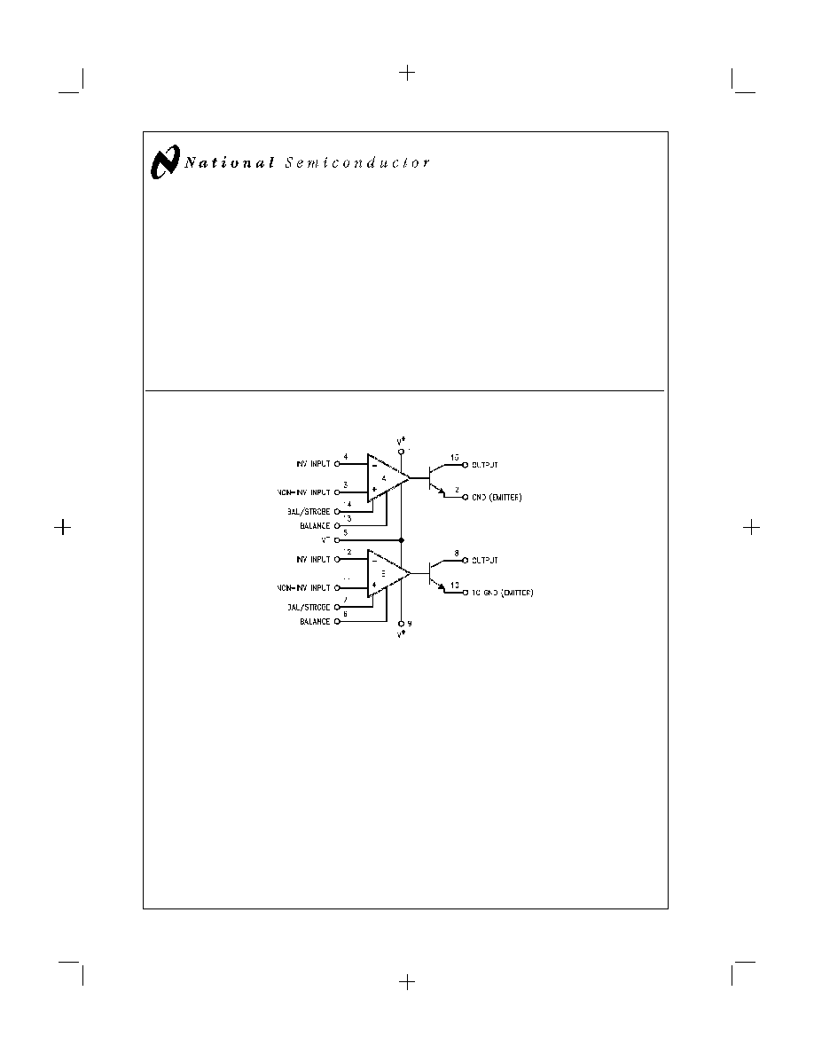
Connection Diagram
DS010116-1
Order Number LH2111D, LH2111D/883 or LH2311D
See NS Package Number D16C
August 1992
LH21
1
1/LH231
1
Dual
V
oltage
Comparators
LH21
1
1/LH231
1
© 1997 National Semiconductor Corporation
DS010116
www.national.com
1
PrintDate=1997/05/02 PrintTime=12:26:32 6564 ds010116 Rev. No. 1
Proof
1
Absolute Maximum Ratings
(Note *NO
TARGET FOR FNXref NS0050*)
If Military/Aerospace specified devices are required,
please contact the National Semiconductor Sales Office/
Distributors for availability and specifications.
Total Supply Voltage (V
+
- V
-
)
36V
Output to Negative Supply Voltage (V
OUT
- V
-
)
50V
Ground to Negative Supply Voltage (GND - V
-
)
30V
Differential Input Voltage
±
30V
Input Voltage (Note 1)
±
15V
Power Dissipation (Note 2)
500 mW
Output Short Circuit Duration
10 sec
Operating Temperature Range LH2111
-55∞C to +125∞C
LH2311
0∞C to +70∞C
Storage Temperature Range
-65∞C to +150∞C
Lead Temperature (Soldering, 10 sec)
300∞C
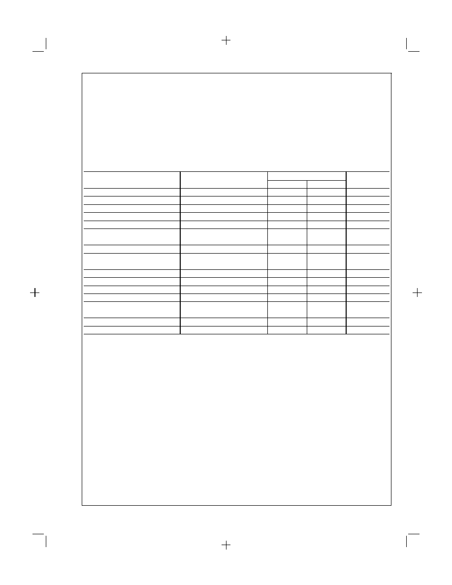
Electrical Characteristics
(Note 3)
Each Side
Parameter
Conditions
Limits
Units
LH2111
LH2311
Input Offset Voltage (Note 4)
T
A
= 25∞C, R
S
50k
3.0
7.5
mV Max
Input Offset Current (Note 4)
T
A
= 25∞C
10
50
nA Max
Input Bias Current
T
A
= 25∞C
100
250
nA Max
Voltage Gain
T
A
= 25∞C
200
200
V/mV Typ
Response Time (Note 5)
T
A
= 25∞C
200
200
ns Typ
Saturation Voltage
V
IN
-5 mV, I
OUT
= 50 mA
1.5
1.5
V Max
T
A
= 25∞C
Strobe On Current
T
A
= 25∞C
3.0
3.0
mA Typ
Output Leakage Current
V
IN
5 mV, V
OUT
= 35V
10
50
nA Max
T
A
= 25∞C
Input Offset Voltage (Note 4)
R
S
50k
4.0
10
mV Max
Input Offset Current (Note 4)
20
70
nA Max
Input Bias Current
150
300
nA Max
Input Voltage Range
±
14
±
14
V Typ
Saturation Voltage
V+
4.5V, V
-
= 0
0.4
0.4
V Max
V
IN
-5 mV, I
SINK
8 mA
Positive Supply Current
T
A
= 25∞C
6.0
7.5
mA Max
Negative Supply Current
T
A
= 25∞C
5.0
5.0
mA Max
Note 1: This rating applies for
±
15V supplies. The positive input voltage limit is 30V above the negative supply. The negative input voltage limit is equal to the nega-
tive supply voltage or 30V below the positive supply, whichever is less.
Note 2: The maximum junction temperature is 150∞C. For operating at elevated temperatures, devices in the flat package, the derating is based on a thermal resis-
tance of 185∞C/W when mounted on a 1/16-inch-thick epoxy glass board with 0.03-inch-wide, 2 ounce copper conductor. The thermal resistance of the dual-in-line
package is 100∞C/W, junction to ambient.
Note 3: These specifications apply for V
S
=
±
15V and -55∞C
T
A
125∞C for the LH2111, and 0∞C
T
A
70∞C for the LH2311, unless otherwise stated. The offset
voltage, offset current and bias current specifications apply for any supply voltage from a single 5V supply up to
±
15V supplies. For the LH2311, V
IN
=
±
10 mV.
Note 4: The offset voltages and offset currents given are the maximum values required to drive the output within a volt of either supply with a 1 mA load. Thus, these
parameters define an error band and take into account the worst case effects of voltage gain and input impedance.
Note 5: The response time specified is for a 100 mV input step with 5 mV overdrive.
Note 6: RETS2111X for the LH2111D and LH2111F military specifications.
PrintDate=1997/05/02 PrintTime=12:26:34 6564 ds010116 Rev. No. 1
Proof
2
www.national.com
2
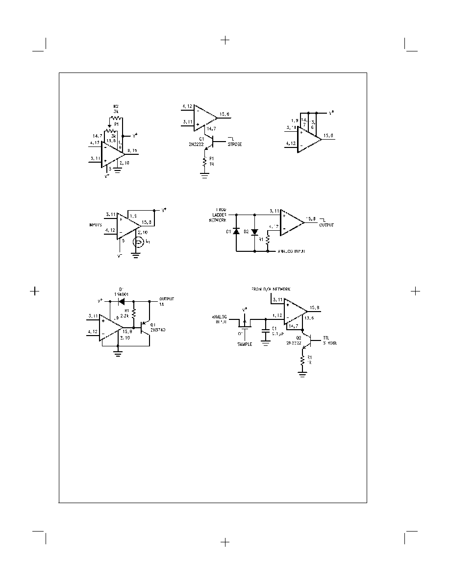
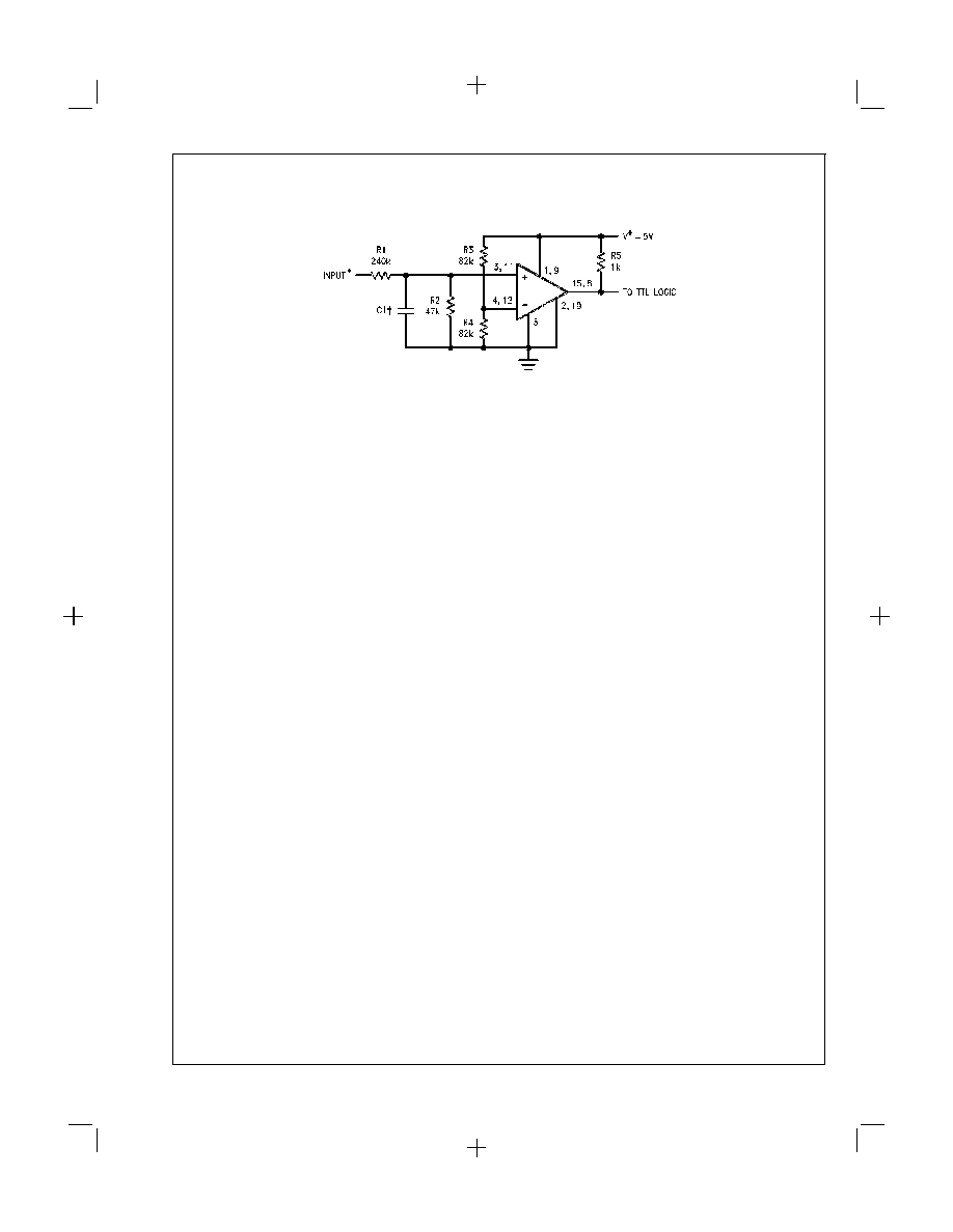
Auxiliary Circuits
Offset Balancing
DS010116-2
Strobing
DS010116-3
Increasing Input Stage
Current
*
DS010116-4
*
Increases typical common mode slew
from 7.0 V/µs to 18 V/µs
Driving Ground-Referred Load
DS010116-5
Using Clamp Diodes to Improve Responses
DS010116-6
Comparator and Solenoid Driver
DS010116-7
Strobing off Both Input
*
and Output Stages
DS010116-8
*
Typical input current is 50 pA with inputs strobed off
3
www.national.com
PrintDate=1997/05/02 PrintTime=12:26:35 6564 ds010116 Rev. No. 1
Proof
3