 | –≠–ª–µ–∫—Ç—Ä–æ–Ω–Ω—ã–π –∫–æ–º–ø–æ–Ω–µ–Ω—Ç: LM1201 | –°–∫–∞—á–∞—Ç—å:  PDF PDF  ZIP ZIP |

TL H 10006
LM1201
Video
Amplifier
System
January 1995
LM1201 Video Amplifier System
General Description
The LM1201 is a wideband video amplifier system intended
for high resolution monochrome or RGB monitor applica-
tions
In addition to the wideband video amplifier the
LM1201 contains a gated differential input black level clamp
comparator for brightness control and an attenuator circuit
for contrast control The LM1201 also contains a voltage
reference for the video input For medium resolution RGB
color monitor applications also see the LM1203 Video Am-
plifier System data sheet
Features
Y
Wideband video amplifier (200 MHz
b
3 dB)
Y
Attenuator circuit for contrast control (
l
40 dB range)
Y
Externally gated comparator for brightness control
Y
Provisions for external gain set and peaking of video
amplifier
Y
Video input voltage reference
Y
Low impedance output driver
Typical Applications
Y
CRT video amplifiers
Y
Video switches
Y
High frequency video preamplifiers
Y
Wideband gain controls
Y
PC monitors
Y
Workstations
Y
Facsimile machines
Y
Printers
Block and Connection Diagram
TL H 10006 ≠ 1
FIGURE 1
Order Number LM1201M or LM1201N
See NS Package Number M16A or N16E
C1996 National Semiconductor Corporation
RRD-B30M56 Printed in U S A

Absolute Maximum Ratings
If Military Aerospace specified devices are required
please contact the National Semiconductor Sales
Office Distributors for availability and specifications
Supply Voltage V
CC
Pins 10 12 15
to Ground Pins 1 7
13 5V
Voltage at Any Input Pin (V
IN
)
V
CC
t
V
IN
t
GND
Video Output Current (I
8
)
28 mA
Package Power Dissipation at T
A
e
25 C
1 56W
(Above 25 C derate based on (i
JA
and T
J
)
Package Thermal Resistance (i
JA
) N16E
80 C W
Package Thermal Resistance (i
JA
) M16A
100 C W
Junction Temperature (T
J
)
150 C
Storage Temperature Range (T
STG
)
b
65 C to
a
150 C
Lead Temperature (Soldering 10 sec )
265 C
ESD Susceptibility
2 kV
Human body model 100 pF discharged through a 1 5 kX
resistor
Operating Ratings
(Note 4)
Temperature Range
0 C to
a
70 C
Supply Voltage (V
CC
)
10 8V
s
V
CC
s
13 2V
Electrical Characteristics
See Test Circuit (Figure 2) T
A
e
25 C V
CC1
e
V
CC2
e
V
CC3
e
12V
DC Static Tests
S9 Open V4
e
6V V5
e
0V V6
e
2 0V unless otherwise stated
Tested
Design
Units
Symbol
Parameter
Conditions
Typical
Limit
Limit
(Limits)
(Note 1)
(Note 2)
I
S
Supply Current
V
CC
Pins 12 15 Only
45
57
mA(max)
V
3
Video Input Reference Voltage
2 65
2 4
V(min)
2 95
V(max)
I
16
Video Input Bias Current
(V
3
≠ V
16
) 10 kX
5 0
20
m
A(max)
V
5L
Clamp Gate Low Input Voltage
Clamp Comparator On
1 2
0 8
V(min)
V
5H
Clamp Gate High Input Voltage
Clamp Comparator Off
1 6
2 0
V(max)
I
5L
Clamp Gate Low Input Current
V
5
e
0V
b
0 5
b
5 0
m
A(max)
I
5H
Clamp Gate High Input Current
V
5
e
12V
0 005
1
m
A(max)
I
2a
Clamp Cap Charge Current
V
2
e
0V
1
0 55
mA(min)
I
2b
Clamp Cap Discharge Current
V
2
e
5V
b
1
b
0 55
mA(min)
V
8L
Video Output Low Voltage
V
2
e
0V
0 5
0 9
V(max)
V
8H
Video Output High Voltage
V
2
e
5V
8 5
8 0
V(min)
V
OS
Comparator Input Offset Voltage
V
6
≠ V
9
g
0 5
g
25
mV(max)
AC Dynamic Tests
S9 Closed V
5
e
0V V
6
e
4V
Symbol
Parameter
Conditions
Typ
Tested
Design
Units
Limit (Note 1)
Limit (Note 2)
(Limits)
Av max
Video Amplifier Gain
V
4
e
12V
8
5 5
V V(min)
D
Av 5V
Attenuation
5V
Ref Av max V
4
e
5V
b
10
dB
D
Av 2V
Attenuation
2V
Ref Av max V
4
e
2V
b
45
dB
THD
Video Amplifier Distortion
V
4
e
5V V
O
e
1 V
p-p
0 3
%
f (
b
3dB)
Video Amplifier Bandwidth (Note 3)
V
4
e
12V V
O
e
100 mV
rms
200
170
MHz(min)
t
r
Output Rise Time (Note 3)
V
O
e
4 V
p-p
2 5
ns
t
f
Output Fall Time (Note 3)
V
O
e
4 V
p-p
3
ns
Note 1
These parameters are guaranteed and 100% production tested
Note 2
Design limits are guaranteed (but not 100% production tested) These limits are not used to calculate outgoing quality levels
Note 3
When measuring video amplifier bandwidth or pulse rise and fall times a double sided full ground plane printed circuit board without socket is recommend-
ed
Note 4
Operating Ratings indicate conditions of which the device is functional but does not guarantee specific performance limits For guaranteed specifications
and test conditions see Electrical Characteristics The guaranteed specifications apply only for the test conditions listed Some performance characteristics may
degrade when the device is not operated under the listed test conditions
http
www national com
2
TL H 10006 ≠ 2
FIGURE 2 LM1201 AC DC Test Circuit
Note
When V
5
s
0 8V and S9 is closed DC feedback around the Video Amplifier is provided by the clamp comparator Under these conditions sine wave or 50%
duty cycle square waves can be used for test purposes The low frequency dominant pole is determined by C2 at Pin 2 Capacitor C9 at pin 9 prevents overloading
the clamp comparator inverting input See applications section for additional information
TL H 10006 ≠ 3
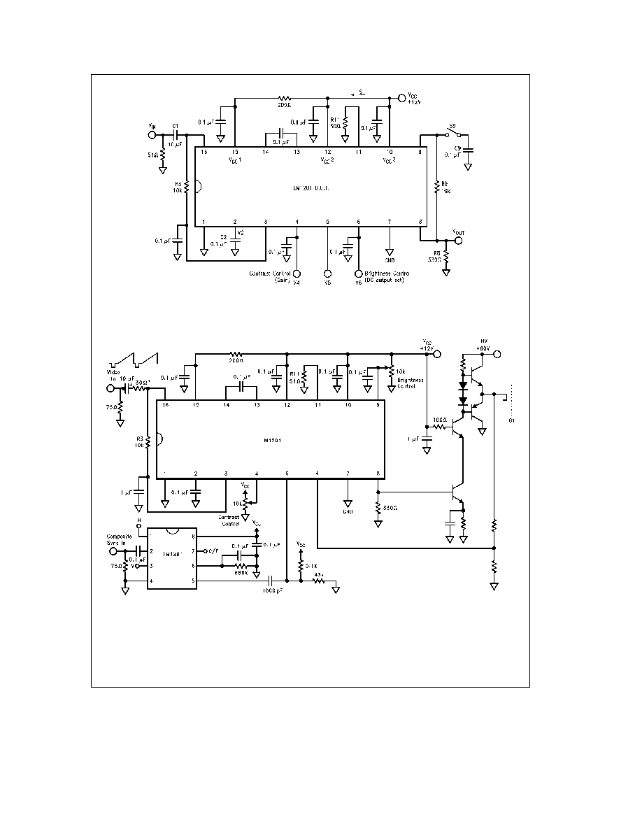
FIGURE 3 Typical Application of the LM1201
30X resistor is added to the input pin for protection against current surges coming from the 10 mF input capacitor By increasing this resistor to well over 100X
the rise and fall times of the LM1201 can be increased for EMI considerations
http
www national com
3

APPLICATIONS INFORMATION
Figure 4 shows the block diagram of a typical analog mono-
chrome monitor The monitor is used with CAD CAM work
stations PCs arcade games and in a wide range of other
applications that benefit from the use of high resolution dis-
play terminals Monitor characteristics may differ in such
ways as sweep rates screen size or in video amplifier
speed but will still be generally configured as shown in
Fig-
ure 4 Separate horizontal and vertical sync signals may be
required or they may be contained as a composite signal in
the video input signal The video input signal is usually
supplied by coaxial cable which is terminated in 75X at the
monitor input and internally AC coupled to the video amplifi-
er The input signal is approximately 1V peak-to-peak in am-
plitude and at the input of the high voltage video section
approximately 6V peak-to-peak At the cathode of the CRT
the video signals can be as high as 60V peak to peak The
block in
Figure 4 labeled ``Video Amplification with DC Con-
trolled Gain Black Level'' contains the function of the
LM1201 video amplifier system
TL H 10006 ≠ 4
FIGURE 4 Typical Monochrome Monitor Block Diagram
http
www national com
4

Circuit Description
Figure 5 is a block diagram of the LM1201 along with the
contrast and brightness controls The contrast control is a
DC operated attenuator which varies the AC gain of the
amplifier without introducing any signal distortions or DC
output shift The brightness control function requires a
``sample and hold'' circuit (black level clamp) which holds
the DC bias of the video amplifier and CRT cathodes con-
stant during the black level reference portion of the video
waveform The clamp comparator when gated on during
this reference period will charge or discharge the clamp
capacitor until the non-inverting input of the clamp compara-
tor matches that of the inverting input voltage which was set
by the brightness control
Figure 6 is a simplified schematic of the LM1201 video am-
plifier along with the recommended external components
The IC pin numbers are circled with all external components
shown outside of the dashed line The video input is applied
to pin 16 via the 10 mF coupling capacitor DC bias to the
video input is through the 10 kX resistor which is connected
to the 2 6V reference at pin 3 The low frequency roll-off of
the amplifier is set by these two components Transistor Q1
buffers the video signal to the base of Q2 The Q2 collector
current is then directed to the V
CC1
supply through Q3 or to
V
CC2
through Q4 and the 500X load resistor depending
upon the differential DC voltage at the bases of Q3 and Q4
The Q3 and Q4 differential base voltage is determined by
the contrast control circuit which is described below The
black level DC voltage at the collector of Q4 is maintained
by Q5 and Q6 which are part of the black level clamp circuit
also described below The video signal appearing at the col-
lector of Q4 is then buffered by Q7 and level shifted down
by Z1 and Q8 to the base of Q9 which will then provide
additional system gain
TL H 10006 ≠ 5
FIGURE 5 Block Diagram of LM201 Video Amplifier with Contrast and Black Level Control
http
www national com
5