TL H 11489
LM1203B
100
MHz
RGB
Video
Amplifier
System
January 1996
LM1203B
100 MHz RGB Video Amplifier System
General Description
The LM1203B is an improved version of the popular
LM1203 wideband video amplifier system The device is in-
tended for high resolution RGB CRT monitors In addition to
three matched video amplifiers the LM1203B contains
three gated differential input black level clamp comparators
for brightness control and three matched attenuator circuits
for contrast control Each video amplifier contains a gain set
or ``Drive'' node for setting maximum system gain or provid-
ing gain trim capability for white balance The LM1203B also
contains a voltage reference for the video inputs The
LM1203B is pin and function compatible with the LM1203
Applications
Y
High resolution RGB CRT monitors
Y
Video AGC amplifiers
Y
Wideband amplifiers with gain and DC offset controls
Features
Y
Three wideband video amplifiers (100 MHz
b
3 dB)
Y
Matched (
g
0 1 dB or 1 2%) attenuators for
contrast control
Y
Three externally gated comparators for
brightness control
Y
Provisions for individual gain control (Drive) of each
video amplifier
Y
Video input voltage reference
Y
Low impedance output driver
Y
Stable on a single sided board
Improvements over LM1203
Y
100 MHz vs 70 MHz bandwidth
Y
V
OUT
low
0 15V vs 0 9V
Y
t
r
t
f
3 7 ns vs 5 ns
Y
Built in power down spot killer
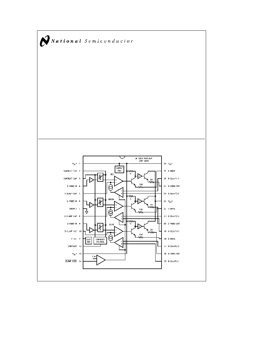
Block and Connection Diagrams
28-Lead Molded DIP
TL H 11489 1
Order Number LM1203BN
See NS Package Number N28B
C1996 National Semiconductor Corporation
RRD-B30M66 Printed in U S A
Absolute Maximum Ratings
(Note 1)
If Military Aerospace specified devices are required
please contact the National Semiconductor Sales
Office Distributors for availability and specifications
Supply Voltage (V
CC
)
Pins 1 13 23 28 (Note 3)
13 5V
Peak Video Output Source Current
(Any 1A) Pins 15 20 or 25
28 mA
Voltage at Any Input Pin (V
IN
)
V
CC
t
V
IN
t
GND
Power Dissipation (P
D
)
(Above 25 C Derate
Based on i
JA
and T
J
)
2 5W
Thermal Resistance (i
JA)
50 C W
Junction Temperature (T
J
)
150 C
ESD Susceptibility (Note 4)
2 0 kV
Storage Temperature
b
65 C to
a
150 C
Lead Temperature
(Soldering 10 seconds)
265 C
Operating Ratings
(Note 2)
Temperature Range
b
20 C to
a
80 C
Supply Voltage (V
CC
)
10 8V
s
V
CC
s
13 2V
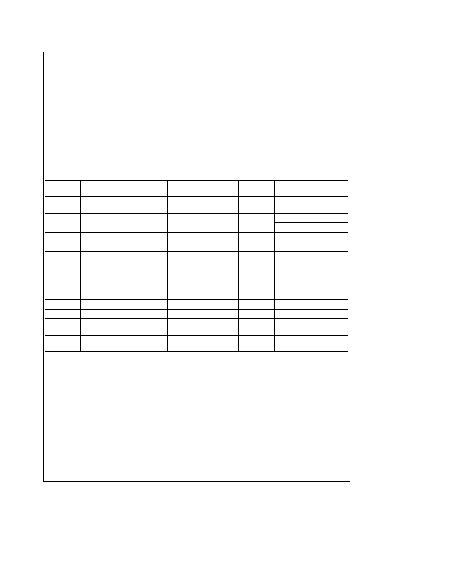
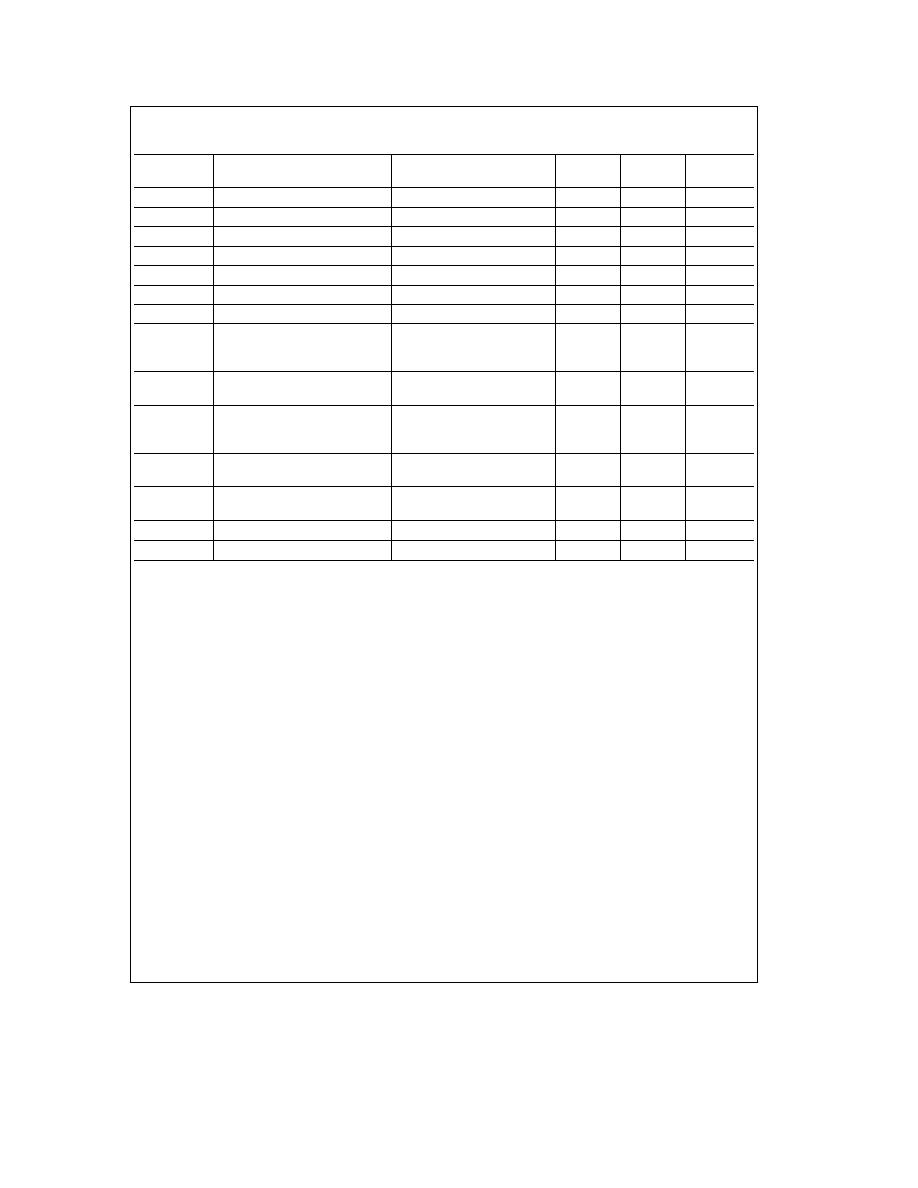
DC Electrical Characteristics
See Test Circuit
(Figure 2) T
A
e
25 C V
CC1
e
V
CC2
e
12V S17 21 26
Open V12
e
6V V14
e
0V V15
e
2 0V unless otherwise stated
Symbol
Parameter
Conditions
Typical
Limit
Units
(Note 5)
(Note 6)
I
S
Supply Current
V
CC1
a
V
CC2
R
L
e
%
70
95
mA(max)
(Note 7)
V11
Video Input Reference Voltage
2 8
2 5
V(min)
3 1
V(max)
I
b
Video Input Bias Current
Any One Amplifier
7
20
m
A(max)
V
14l
Clamp Gate Low Input Voltage
Clamp Comparators On
1 2
0 8
V(max)
V
14h
Clamp Gate High Input Voltage
Clamp Comparators Off
1 6
2 0
V(min)
I
14l
Clamp Gate Low Input Current
V14
e
0V
b
1
b
5 0
m
A(max)
I
14h
Clamp Gate High Input Current
V14
e
12V
0 07
0 2
m
A(max)
I
clampa
Clamp Cap Charge Current
V5 8 or 10
e
0V
750
500
m
A(min)
I
clampb
Clamp Cap Discharge Current
V5 8 or 10
e
5V
b
750
500
m
A(min)
V
OL
Video Output Low Voltage
V5 8 or 10
e
0V
0 15
0 5
V(max)
V
OH
Video Output High Voltage
V5 8 or 10
e
5V
7 5
7
V(min)
D
V
O(2V)
Video Output Offset Voltage
Between Any Two
2
g
25
mV(max)
Amplifiers V15
e
2V
D
V
O(4V)
Video Output Offset Voltage
Between Any Two
2
g
25
mV(max)
Amplifiers V15
e
4V
http
www national com
2
AC Electrical Characteristics
See Test Circuit
(Figure 2) T
A
e
25 C V
CC1
e
V
CC2
e
12V S17 21 26
Closed V14
e
0V V15
e
4V unless otherwise stated
Symbol
Parameter
Conditions
Typical
Limit
Units
(Note 5)
(Note 6)
A
V max
Video Amplifier Gain
V12
e
12V V
IN
e
560 mV
PP
6 5
4 5
V V(min)
D
V
V 5V
Attenuation
5V
Ref A
V max
V12
e
5V
b
8
dB
D
A
V 2V
Attenuation
2V
Ref A
V max
V12
e
2V
b
30
dB
A
V match
Absolute Gain Match
A
V
max
V12
e
12V (Note 8)
g
0 3
dB
D
A
V track 1
Gain Change between Amplifiers
V12
e
5V (Notes 8 9)
g
0 1
dB
D
A
V track 2
Gain Change between Amplifiers
V12
e
2V (Notes 8 9)
g
0 3
dB
THD
Video Amplifier Distortion
V12
e
3V V
O
e
1 V
PP
1
%
f (
b
3 dB)
Video Amplifier Bandwidth
V12
e
12V V
O
e
4 V
PP
(Notes 10 11)
(With 36 pF Peaking Cap from
100
MHz
Pins 18 22 and 27 to GND)
f (
b
3 dB)
Video Amplifier Bandwidth
V12
e
12V V
O
e
4 V
PP
60
MHz
(Notes 10 11)
(No External Peaking Cap)
t
r
t
f
Output Rise Fall Time
V
O
e
4 V
PP
(With 36 pF
(Note 10)
Peaking Cap from Pins 18
3 7
ns
22 and 27 to GND)
t
r
Output Rise Time (Note 10)
V
O
e
4 V
PP
(No External
5 5
ns
Peaking Capacitor)
t
f
Output Fall Time (Note 10)
V
O
e
4 V
PP
(No External
6 0
ns
Peaking Capacitor)
V
sep 10 kHz
Video Amplifier 10 kHz Isolation
V12
e
12V (Note 12)
b
70
dB
V
sep 10 MHz
Video Amplifier 10 MHz Isolation
V12
e
12V (Notes 10 12)
b
50
dB
Note 1
Absolute Maximum Ratings indicate limits beyond which damage to the device may occur
Note 2
Operating Ratings indicate conditions for which the device is functional but do not guarantee specific performance limits For guaranteed specifications
and test conditions see the Electrical Characteristics The guaranteed specifications apply only for the test conditions listed Some performance characteristics
may degrade when the device is not operated under the listed test conditions
Note 3
V
CC
supply pins 1 13 23 28 must be externally wired together to prevent internal damage during V
CC
power on off cycles
Note 4
Human body model 100 pF discharged through a 1 5 kX resistor
Note 5
Typical specifications are specified at
a
25 C and represent the most likely parametric norm
Note 6
Tested limits are guaranteed to National's AOQL (Average Outgoing Quality Level)
Note 7
The supply current specified is the quiescent current for V
CC1
and V
CC2
with R
L
e
%
see
Figure 2 's test circuit The supply current for V
CC2
(pin 23) also
depends on the output load With video output at 2V DC the additional current through V
CC2
is 18 mA for
Figure 2 's test circuit
Note 8
Measure gain difference between any two amplifiers V
IN
e
1 V
PP
Note 9 D
A
V
track is a measure of the ability of any two amplifiers to track each other and quantifies the matching of the three attenuators It is the difference in
gain change between any two amplifiers with the contrast voltage (V12) at either 5V or 2V measured relative to an A
V
max condition V12
e
12V For example at
A
V
max the three amplifiers' gains might be 17 4 dB 16 9 dB and 16 4 dB and change to 7 3 dB 6 9 dB and 6 5 dB respectively for V12
e
5V This yields the
measured typical
g
0 1 dB channel tracking
Note 10
When measuring video amplifier bandwidth or pulse rise and fall times a single sided with ground plane printed circuit board without socket is
recommended Video amplifier 10 MHz isolation test also requires this printed circuit board
Note 11
Adjust input frequency from 10 kHz (A
V
max reference level) to the
b
3 dB corner frequency (f
b
3 dB
)
Note 12
Measure output levels of the other two undriven amplifiers relative to the driven amplifier to determine channel separation Terminate the undriven
amplifier inputs to simulate generator loading Repeat test at f
IN
e
10 MHz for V
sep
e
10 MHz
http
www national com
3