 | –≠–ª–µ–∫—Ç—Ä–æ–Ω–Ω—ã–π –∫–æ–º–ø–æ–Ω–µ–Ω—Ç: LM1236 | –°–∫–∞—á–∞—Ç—å:  PDF PDF  ZIP ZIP |
LM1236
150 MHz I
2
C Compatible RGB Preamplifier with Internal
254 Character OSD ROM, 512 Character RAM and 4
DACs
General Description
The LM1236 pre-amp is an integrated CMOS CRT preamp.
It has an I
2
C compatible interface which allows control of all
the parameters necessary to directly setup and adjust the
gain and contrast in the CRT display. Brightness and bias
can be controlled through the DAC outputs, which are well
matched to the LM2479 and LM2480 integrated bias clamp
ICs. The LM1236 preamp is also designed to be compatible
with the LM246x high gain driver family.
Black level clamping of the video signal is carried out directly
on the AC coupled input signal into the high impedance
preamplifier input, thus eliminating the need for additional
clamp capacitors. Horizontal and vertical blanking of the
outputs is provided. Vertical blanking is optional and its
duration is register programmable.
The IC is packaged in an industry standard 24-lead DIP
molded plastic package.
Features
n
Internal 254 character OSD ROM usable as either (a)
190 2-color plus 64 4-color characters, (b) 318 2-color
characters, or (c) some combination in between
n
Internal 512 character RAM, which can be displayed as
one single or two independent windows
n
Enhanced I
2
C compatible microcontroller interface
to allow versatile Page RAM access
n
OSD Window Fade In/Fade Out
n
OSD Half Tone Transparency
n
OSD override allows OSD messages to override video
and the use of burn-in screens with no video output.
n
4 DAC outputs (8-bit resolution) for bus controlled CRT
bias and brightness
n
Spot killer which blanks the video outputs when V
CC
falls below the specified threshold
n
Suitable for use with discrete or integrated clamp, with
software configurable brightness mixer
n
4-Bit Programmable start position for internal
Horizontal Blanking
n
Horizontal blanking and OSD synchronization directly
from deflection signals. The blanking can be disabled, if
desired.
n
Vertical blanking and OSD synchronization directly from
deflection signals. The blanking width is register
programmable and can be disabled, if desired.
n
Power Saving Mode with 65% power reduction
n
Matched to LM246x driver and LM2479/80 bias IC's
Applications
n
Low end 15" and 17" bus controlled monitors with OSD
n
1024x768 displays up to 85 Hz requiring OSD capability
n
Very low cost systems with LM246x driver
PRELIMINARY
September 2003
LM1236
150
MHz
I
2
C
Compatible
RGB
Preamplifier
with
Internal
254
Character
OSD
ROM,
512
Character
RAM
and
4
DACs
© 2005 National Semiconductor Corporation
DS200757
www.national.com

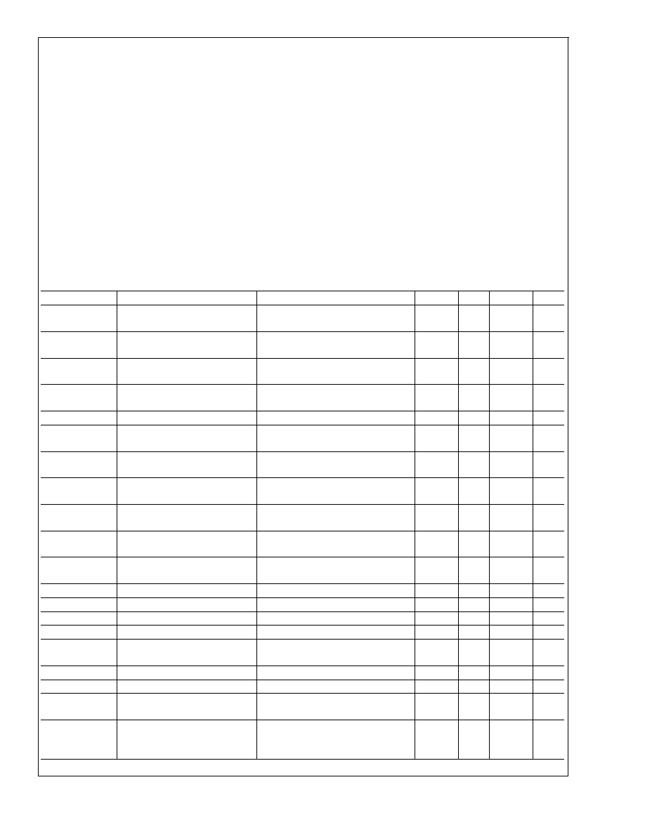
Internal Block Diagram
20075701
FIGURE 1. Order Number LM1236AAA/NA
See NS Package Number N24D
LM1236
www.national.com
2
Absolute Maximum Ratings
(Notes 1, 3)
If Military/Aerospace specified devices are required, please contact the National Semiconductor Sales Office/
Distributors for availability and specifications.
Supply Voltage V
CC
, Pins 10 and 18
6.0V
Peak Video DC Output Source Current
(Any One Amp) Pins 19, 20 or 21
1.5 mA
Voltage at Any Input Pin (V
IN
)
V
CC
+0.5
V
IN
-0.5V
Video Inputs (pk-pk)
0.0
V
IN
1.2V
Thermal Resistance to Ambient (
JA
)
51∞C/W
Power Dissipation (P
D
)
(Above 25∞C Derate Based
on
JA
and T
J
)
2.4W
Thermal Resistance to Case (
JC
)
32∞C/W
Junction Temperature (T
J
)
150∞C
ESD Susceptibility (Note 4)
3.0 kV
ESD Machine Model (Note 13)
350V
Storage Temperature
-65∞C to +150∞C
Lead Temperature (Soldering, 10 sec.)
265∞C
Operating Ratings
(Note 2)
Temperature Range
0∞C to +70∞C
Supply Voltage V
CC
4.75V
V
CC
5.25V
Video Inputs (pk-pk)
0.0V
V
IN
1.0V
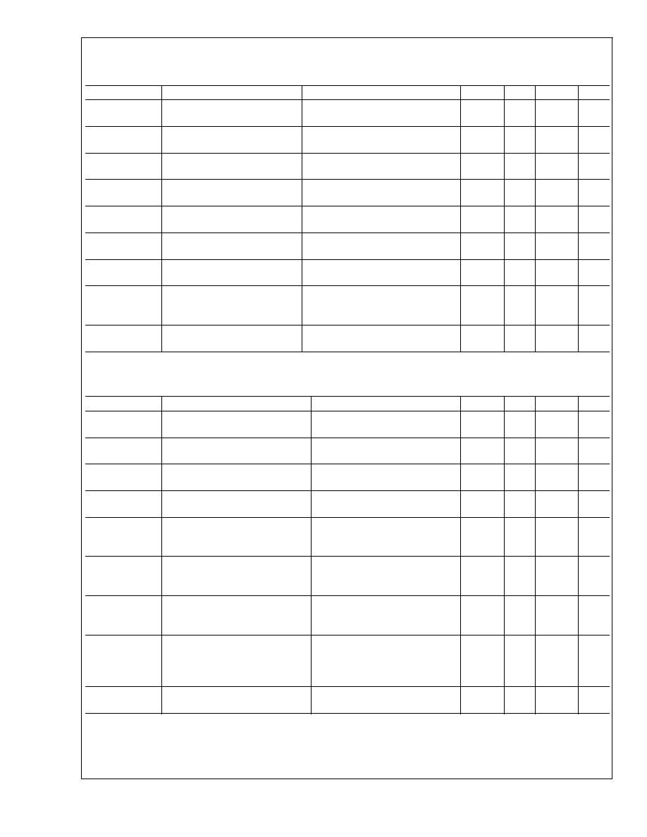
Video Signal Electrical Characteristics
Unless otherwise noted: T
A
= 25∞C, V
CC
= +5.0V, V
IN
= 0.70 V
P-P
, V
ABL
= V
CC
, C
L
= 8 pF, Video Outputs = 2.0 V
P-P
. Setting
numbers refer to the definitions in Table 1. See (Note 7) for Min and Max parameters and (Note 6) for Typicals.
Symbol
Parameter
Conditions
Min
Typ
Max
Units
I
S
Supply Current
Test Setting 1, both supplies, no
output loading. See (Note 8).
200
250
mA
I
S-PS
Supply Current, Power Save
Mode
Test Setting 1, both supplies, no
output loading. See (Note 8).
70
95
mA
V
O BLK
Active Video Black Level Output
Voltage
Test Setting 4, no AC input signal, DC
offset (register 0x8438 set to 0xd5).
1.2
VDC
V
O BLK STEP
Active Video Black Level Step
Size
Test Setting 4, no AC input signal.
100
mVDC
V
O
Max
Maximum Video Output Voltage
Test Setting 3, Video in = 0.70 V
P-P
4.0
4.3
V
LE
Linearity Error
Test Setting 4, staircase input signal.
See(Note 9)
5
%
t
r
Video Rise Time
(Note 5), 10% to 90%, Test Setting 4,
AC input signal.
3.1
ns
OS
R
Rising Edge Overshoot
(Note 5), Test Setting 4, AC input
signal.
2
%
t
f
Video Fall Time
(Note 5), 90% to 10%, Test Setting 4,
AC input signal.
2.9
ns
OS
F
Falling Edge Overshoot
(Note 5), Test Setting 4, AC input
signal.
2
%
BW
Channel Bandwidth (-3 dB)
(Note 5), Test Setting 4, AC input
signal.
150
MHz
V
SEP
10 kHz
Video Amplifier 10 kHz Isolation
(Note 14), Test Setting 8.
-60
dB
V
SEP
10 MHz
Video Amplifier 10 MHz Isolation
(Note 14), Test Setting 8.
-50
dB
A
V
Max
Maximum Voltage Gain
Test Setting 8, AC input signal.
3.8
4.1
V/V
A
V
C-50%
Contrast Attenuation
@
50%
Test Setting 5, AC input signal.
-5.2
dB
A
V
Min/A
V
Max
Maximum Contrast Attenuation
(dB)
Test Setting 2, AC input signal.
-20
dB
A
V
G-50%
Gain Attenuation
@
50%
Test Setting 6, AC input signal.
-4.0
dB
A
V
G-Min
Maximum Gain Attenuation
Test Setting 7, AC input signal.
-11
dB
A
V
Match
Maximum Gain Match between
Channels
Test Setting 3, AC input signal.
±
0.5
dB
A
V
Track
Gain Change between Channels
Tracking when changing from Test
Setting 8 to Test Setting 5. See (Note
11).
±
0.5
dB
LM1236
www.national.com
3
Video Signal Electrical Characteristics
(Continued)
Unless otherwise noted: T
A
= 25∞C, V
CC
= +5.0V, V
IN
= 0.70 V
P-P
, V
ABL
= V
CC
, C
L
= 8 pF, Video Outputs = 2.0 V
P-P
. Setting
numbers refer to the definitions in Table 1. See (Note 7) for Min and Max parameters and (Note 6) for Typicals.
Symbol
Parameter
Conditions
Min
Typ
Max
Units
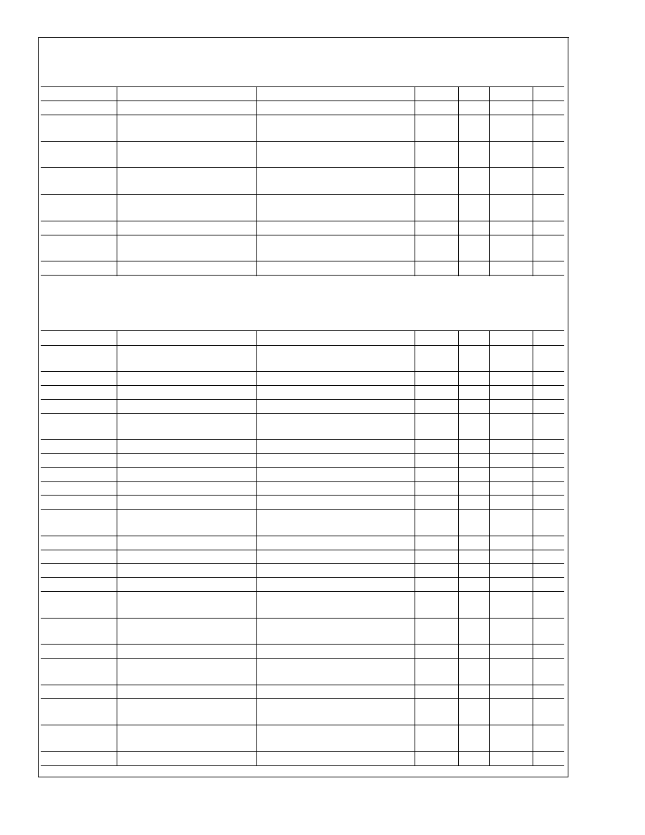
V
ABL
TH
ABL Control Range Upper Limit
(Note 12), Test Setting 4, AC input
signal.
4.8
V
V
ABL
Range
ABL Gain Reduction Range
(Note 12), Test Setting 4, AC input
signal.
2.8
V
A
V 3.5
/A
V Max
ABL Gain Reduction at 3.5V
(Note 12), Test Setting 4, AC input
signal. V
ABL
= 3.5V
-2
dB
A
V 2.0
/A
V Max
ABL Gain Reduction at 2.0V
(Note 12), Test Setting 4, AC input
signal. V
ABL
= 2.0V
-12
dB
I
ABL
Active
ABL Input Bias Current during
ABL
(Note 12), Test Setting 4, AC input
signal. V
ABL
= V
ABL
MIN GAIN
µA
I
ABL
Max
ABL Input Current Sink Capability (Note 12), Test Setting 4, AC input
signal.
1.0
mA
V
ABL
Max
Maximum ABL Input Voltage
during Clamping
(Note 12), Test Setting 4, AC input
signal. I
ABL
= I
ABL
MAX
V
CC
+
0.1
V
A
V
ABL Track
ABL Gain Tracking Error
(Note 9), Test Setting 4, 0.7 V
P-P
input signal, ABL voltage set to 4.5V
and 2.5V.
4.5
%
R
IP
Minimum Input Resistance (pins
5, 6, 7)
Test Setting 4.
20
M
OSD Electrical Characteristics
Unless otherwise noted: T
A
= 25∞C, V
CC
= +5.0V. See (Note 7) for Min and Max parameters and (Note 6) for Typicals.
Symbol
Parameter
Conditions
Min
Typ
Max
Units
V
OSDHIGH
max
Maximum OSD Level with OSD
Contrast 11
Palette Set at 111, OSD Contrast =
11, Test Setting 3
4.5
V
V
OSDHIGH
10
Maximum OSD Level with OSD
Contrast 10
Palette Set at 111, OSD Contrast =
10, Test Setting 3
3.9
V
V
OSDHIGH
01
Maximum OSD Level with OSD
Contrast 01
Palette Set at 111, OSD Contrast =
01, Test Setting 3
3.2
V
V
OSDHIGH
00
Maximum OSD Level with OSD
Contrast 00
Palette Set at 111, OSD Contrast =
00, Test Setting 3
2.4
V
V
OSD
(Black)
Difference between OSD Black
Level and Video Black Level (same
channel)
Register 08=0x18, Input Video =
Black, Same Channel, Test Setting
8
20
mV
V
BL,OSD-Video
(Ch-Ch)
Difference between OSD Black
Level and Video Black Level
between any two channels
Register 08=0x18, Input Video =
Black, Same Channel, Same
Channel, Test Setting 8
20
mV
V
OSD
(White)
Output Match between Channels
Palette Set at 111, OSD Contrast =
11, Maximum difference between R,
G, and B
3
%
V
OSD
/V
Video
(White)
Matching of OSD to Video peak to
peak amplitude ratios between
channels, normalized to the
smallest ratio.
Palette Set at 111, OSD Contrast =
10, Test Setting 4
3
%
V
OSD-out
(Track)
Output Variation between Channels OSD contrast varied from max to
min
3
%
LM1236
www.national.com
4
DAC Output Electrical Characteristics
Unless otherwise noted: T
A
= 25∞C, V
CC
= +5.0V, V
IN
= 0.7V, V
ABL
= V
CC
, C
L
= 8 pF, Video Outputs = 2.0 V
P-P
. See (Note 7)
for Min and Max parameters and (Note 6) for Typicals. DAC parameters apply to all 4 DACs.
Symbol
Parameter
Conditions
Min
Typ
Max
Units
V
Min DAC
Min Output Voltage of DAC
Register Value = 0x00
0.5
0.7
V
V
Max DAC
Mode 00
Max Output Voltage of DAC
Register Value = 0xFF,
DCF[1:0] = 00b
4.2
V
V
Max DAC
Mode 01
Max Output Voltage of DAC in
DCF Mode 01
Register Value = 0xFF,
DCF[1:0] = 01b
2.35
V
V
Max DAC
(Temp)
DAC Output Voltage Variation
with Temperature
0
<
T
<
70∞C ambient
±
0.5
mV/∞C
V
Max DAC
(V
CC
)
DAC Output Voltage Variation
with V
CC
V
CC
varied from 4.75V to 5.25V, DAC
register set to mid-range (0x7F)
50
mV
Linearity
Linearity of DAC over its Range
5
%
Monotonicity
Monotonicity of the DAC
Excluding Dead Zones
±
0.5
LSB
I
MAX
Max Load Current
1.0
mA
System Interface Signal Characteristics
Unless otherwise noted: T
A
= 25∞C, V
CC
= +5.0V, V
IN
= 0.7V, V
ABL
= V
CC
, C
L
= 8 pF, Video Outputs = 2.0 V
P-P
. See (Note 7)
for Min and Max parameters and (Note 6) for Typicals. DAC parameters apply to all 4 DACs.
Symbol
Parameter
Conditions
Min
Typ
Max
Units
V
VTH+
VFLYBACK Positive Switching
Guarantee
Vertical Blanking triggered
2.0
V
V
SPOT
Spot Killer Voltage
Table 14, V
CC
Adjusted to Activate
3.4
3.9
4.3
V
V
Ref
V
Ref
Output Voltage (pin 2)
1.25
1.45
1.65
V
V
IL
(SCL, SDA)
Logic Low Input Voltage
-0.5
1.5
V
V
IH
(SCL, SDA)
Logic High Input Voltage
3.5
V
CC
+
0.5
V
I
L
(SCL, SDA)
Logic Low Input Current
SDA or SCL, Input Voltage = 0.4V
±
10
µA
I
H
(SCL, SDA)
Logic High Input Voltage
SDA or SCL, Input Voltage = 4.5V
±
10
µA
V
OL
(SCL, SDA)
Logic Low Output Voltage
I
O
= 3 mA
0.5
V
f
H
Min
Minimum Horizontal Frequency
PLL & OSD Functioning; PPL = 0
25
kHz
f
H
Max
Maximum Horizontal Frequency
PLL & OSD Functioning; PPL = 4
110
kHz
I
HFB IN
Max
Horizontal Flyback Input
Current Absolute Maximum during
Flyback
5
mA
I
IN
Peak Current during Flyback
Design Value
4
mA
I
HFB OUT
Max
Horizontal Flyback Input Current
Absolute Maximum during Scan
-700
µA
I
OUT
Peak Current during Scan
Not exact - Duty Cycle Dependent
-550
µA
I
IN THRESHOLD
I
IN
H-Blank Detection Threshold
0
µA
t
H-BLANK ON
H-Blank Time Delay - On
+ Zero crossing of I
HFB
to 50% of
output blanking start. I
24
= +1.5mA
45
ns
t
H-BLANK OFF
H-Blank Time Delay - Off
- Zero crossing of I
HFB
to 50% of
output blanking end. I
24
= -100µA
85
ns
V
BLANK
Max
Maximum Video Blanking Level
Test Setting 4, AC input signal
0
0.25
V
f
FREERUN
Free Run H Frequency, Including
H Blank
42
kHz
t
PW CLAMP
Minimum Clamp Pulse Width
See (Note 15)
200
ns
V
CLAMP MAX
Maximum Low Level Clamp
Pulse Voltage
Video Clamp Functioning
2.0
V
V
CLAMP MIN
Minimum High Level Clamp
Pulse Voltage
Video Clamp Functioning
3.0
V
I
CLAMP
Low
Clamp Gate Low Input Current
V
23
= 2V
-0.4
µA
LM1236
www.national.com
5