 | –≠–ª–µ–∫—Ç—Ä–æ–Ω–Ω—ã–π –∫–æ–º–ø–æ–Ω–µ–Ω—Ç: LM1295 | –°–∫–∞—á–∞—Ç—å:  PDF PDF  ZIP ZIP |

LM1295
DC Controlled Geometry Correction System for
Continuous Sync Monitors
General Description
The LM1295 is specifically designed for use in a continuous
sync monitor. The injection-locked vertical oscillator oper-
ates from 50 Hz to 170 Hz, covering all known video moni-
tors. A differential output current is provided in order to pre-
vent ground interaction.
The IC provides two outputs composed of the summation of
DC controlled 1st and 2nd order output terms. The first out-
put corrects for EW pincushion and trapezoid. The second
corrects for parallelogram and bow.
A DC controlled output is provided for vertical dynamic focus
correction.
The IC is packaged in a 24-pin narrow DIP package and op-
erates on a single 12V power supply.
Features
n
Vertical scanning frequency 50 Hz≠170 Hz
n
DC controlled correction term amplitudes
n
Up to 125 kHz bandwidth for dynamic input signals
n
Minimum external parts count
n
Multiple IC connection for convergence applications
flexibility
n
Stable vertical amplitude over temperature
n
Compatible with the LM1291 Horizontal PLL in a H/V
system
n
Dynamic vertical deflection correction for second anode
high voltage drop
n
Both positive and negative going correction signals
Connection Diagram
DS012324-1
FIGURE 1. Order Number LM1295N
See NS Package Number N24C
April 1999
LM1295
DC
Controlled
Geometry
Correction
System
for
Continuous
Sync
Monitors
© 1999 National Semiconductor Corporation
DS012324
www.national.com
Absolute Maximum Ratings
(Notes 1, 3)
If Military/Aerospace specified devices are required,
please contact the National Semiconductor Sales Office/
Distributors for availability and specifications.
Supply Voltage
15V
Input Voltage
(DC, pins 2, 4, 6, 10, 11, 12, 13, 15)
5V
Input Voltage (AC, Pin 4)
5 V
PP
Power Dissipation (Note 4)
(Above 25∞C Derate Based on
JA
and T
J
)
1.8W
Thermal Resistance (
JA
)
70∞C/W
Junction Temperature (T
J
)
150∞C
ESD Susceptibility (Note 5)
1.8 kV
Storage Temperature
-65∞C to +150∞C
Lead Temperature (Soldering, 10 sec.)
265∞C
Operating Ratings
(Note 2)
Operating Temperature Range
-20∞C to +80∞C
Supply Voltage (V
CC
)
10.8V
V
CC
13.2V
Input Voltage
(DC, pins 2, 4, 6, 10, 11, 12,
13, 15)
4V
Input Voltage
(AC, pin 4)
4 V
PP
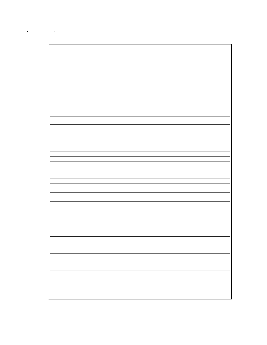
Electrical Characteristics
See Test Circuit (
Figure 2); T
A
= 25∞C; V
CC
= 12V.
Symbol
Parameter
Conditions
Typical
(Note 6)
Limit
(Note 7)
Units
I
CC
Supply Current
All Control Inputs = 3V
25
35
mA
(max)
V
REF
Internal Ref Voltage at Pin 8
8.2
V
R
IN
Input Resistance
Pins 6, 10≠13, 15
50
30
k
(min)
F
FR
Free-Run Frequency
45
Hz
F
max
Maximum Frequency
170
Hz
Cntlbw
Control Inputs Bandwidth
Pins 6, 10≠13, 15
125
kHz
V
HTS
Vertical Height Temperature
Stability
V Height = 4V, V Dyn Height = 3V,
F = 100 Hz, T
A
= 0∞C to 70∞C (Note 9)
1
%
V
DIFF
Vertical Differential Output Current
V Height = 4V, V Dyn Height = 4V,
Pin 24 Minus Pin 23
1
mA(min)
V
SYNH
V Sync High Input Voltage
2.4
V(min)
V
SYNL
V Sync Low Input Voltage
0.8
V
(max)
V
CMRR
Vertical Output CMRR
V
O
= 1V to 4V, V Height = 2V,
V Dyn Height = 3V
30
dB
V
PSRR
Vertical Output PSSR
V
CC
= 10.8V to 13.2V, V Height = 2V,
V Dyn Height = 3V
30
dB
V
OP-P
Vertical Peak Output Voltage
R
L
= 10k
6
5
V
PP
(min)
V
RERR
Vertical Ramp Distortion
(Note 8) V Height = 4V,
V Dyn Height = 3V
1
%
V
SOERR
Vertical Parabola Distortion
(Note 9) V Height = 2.2V, F = 100 Hz,
V Dyn Height = 3V
8
%
CR
FO
First Order (Ramp) Correction,
H Dyn Cntr (Pin 14)
Pin 12 = 0V
Pin 12 = 4V
V Dyn Height = 3V, V Height = 4V,
Parabola Nulled
2.50
2.25
V
PP
CR
FO
First Order (Ramp) Correction,
H Dyn Width (Pin 19)
Pin 11 = 0V
Pin 11 = 4V
V Dyn Height = 3V, V Height = 4V,
Parabola Nulled
0.85
0.75
V
PP
CP
SO
Parabola Correction Range,
H Dyn Cntr (Pin 14),
H Dyn Width (Pin 9),
V Dyn Focus (Pin 16)
Pins 10, 13, 15 = 0V
Pins 10, 13, 15 = 4V
V Dyn Height = 3V, V Height = 4V,
Ramp Nulled for H Dyn Cntr and H Dyn
Width
1.2
1.0
V
PP
www.national.com
2
Electrical Characteristics
(Continued)
See Test Circuit (
Figure 2); T
A
= 25∞C; V
CC
= 12V.
Symbol
Parameter
Conditions
Typical
(Note 6)
Limit
(Note 7)
Units
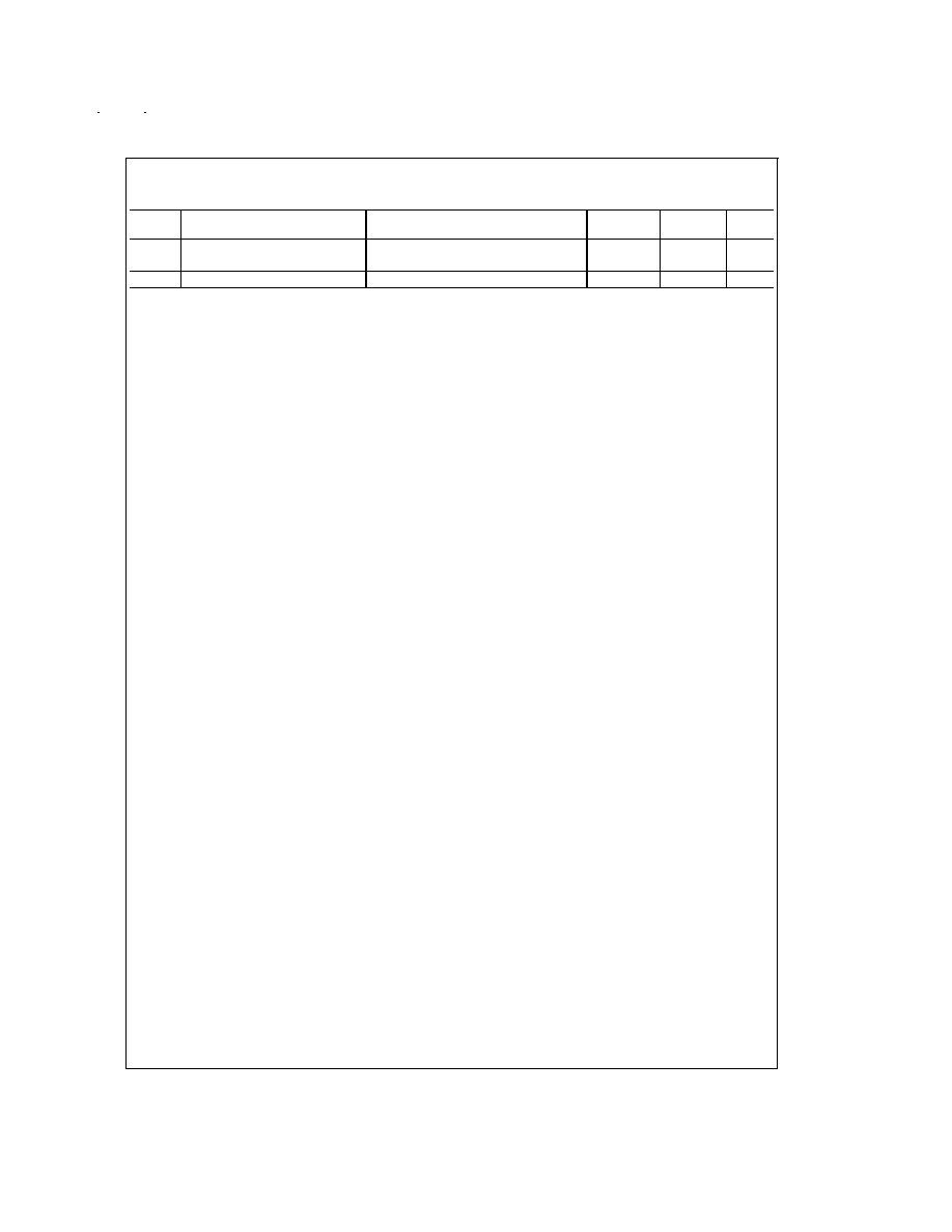
V
ODC
Output DC Bias
Pins 9, 14 and 16; All Control
Inputs at 2.2V
4.0
V
DC
I
O
Output Current
Pins 9, 14 and 16
5.0
mA
Note 1: Absolute Maximum Ratings indicate limits beyond which damage to the device may occur.
Note 2: Operating Ratings indicate conditions for which the device is functional, but do not guarantee specific performance limits. For guaranteed specifications and
test conditions, see the Electrical Characteristics. The guaranteed specifications apply only for the test conditions listed. Some performance characteristics may de-
grade when the device is not operated under the listed test conditions.
Note 3: All voltages are measured wIth respect to GND, unless otherwise specified.
Note 4: The maximum power dissipation must be derated at elevated temperatures and is dictated by T
Jmax
,
JA
and the ambient temperature, T
A
. The maximum
allowable power dissipation at any temperature is P
D
= (T
Jmax
- T
A
)/
JA
or the number given in the Absolute Maximum Ratings, whichever is lower. For this device,
T
Jmax
= 150∞C. The typical thermal resistance (
JA
) of these parts when board mounted follow: LM1295N 70∞C/W.
Note 5: Human body model, 100 pF capacitor discharged through a 1.5 k
resistor.
Note 6: Typicals are at T
A
= T
J
= 25∞C and represent most likely parametric norm.
Note 7: Tested limits are guaranteed to National's AOQL (Average Outgoing Quality Level).
Note 8: The deviation from a straight line drawn through measured points at 5% and 95% of the ramp is used to calculate distortion.
Distortion = 100 (deviation, volts)/(95% value - 5% value, volts). Deviations are measured at
1
/
3
and
2
/
3
of the ramp time period.
Note 9: The deviation from a theoretical parabola drawn through the apex of the actual parabola is used to calculate distortion.
Distortion = 100 (deviation, volts)/(theoretical parabola, volts) at measuring point. Nine points are measured.
Note 10: The amplitude stability versus temperature is typically 1% or less at 100 Hz when a standard 10k 5%
1
/
4
W carbon film resistor is connected between pins
21 and 22 and located close to the package. The negative temperature coefficient of the resistor corrects for the negative temperature coefficient of the LM1295. The
typical amplitude stability of the LM1295 by itself is 2%.
www.national.com
3

Test Circuit
Typical Performance Characteristics
T
A
= 25∞C, V
Height
= 0V to 4V, V
Dyn Height
= 3V
DS012324-2
FIGURE 2.
Lowest Lock Frequency vs OSC Cap
DS012324-12
Graph 1
www.national.com
4

Typical Performance Characteristics
T
A
= 25∞C, F = 100 Hz, V
Height
= 4V, V
Dyn Height
= 3V, Test
Circuit --
Figure 2
H Dyn Width Output (Pin 9)
DS012324-10
H Dyn Width Output (Pin 9)
DS012324-11
H Dyn Width Output (Pin 9)
DS012324-13
H Dyn Width Output (Pin 9)
DS012324-14
H Dyn Ctr Output (Pin 14)
DS012324-15
H Dyn Ctr Output (Pin 14)
DS012324-16
www.national.com
5