 | –≠–ª–µ–∫—Ç—Ä–æ–Ω–Ω—ã–π –∫–æ–º–ø–æ–Ω–µ–Ω—Ç: LM12CLK | –°–∫–∞—á–∞—Ç—å:  PDF PDF  ZIP ZIP |
LM12CL
80W Operational Amplifier
General Description
The LM12 is a power op amp capable of driving
±
25V at
±
10A while operating from
±
30V supplies. The monolithic IC
can deliver 80W of sine wave power into a 4
load with
0.01% distortion. Power bandwidth is 60 kHz. Further, a
peak dissipation capability of 800W allows it to handle reac-
tive loads such as transducers, actuators or small motors
without derating. Important features include:
∑
input protection
∑
controlled turn on
∑
thermal limiting
∑
overvoltage shutdown
∑
output-current limiting
∑
dynamic safe-area protection
The IC delivers
±
10A output current at any output voltage
yet is completely protected against overloads, including
shorts to the supplies. The dynamic safe-area protection is
provided by instantaneous peak-temperature limiting within
the power transistor array.
The turn-on characteristics are controlled by keeping the
output open-circuited until the total supply voltage reaches
14V. The output is also opened as the case temperature ex-
ceeds 150∞C or as the supply voltage approaches the
BV
CEO
of the output transistors. The IC withstands overvolt-
ages to 80V.
This monolithic op amp is compensated for unity-gain feed-
back, with a small-signal bandwidth of 700 kHz. Slew rate is
9V/µs, even as a follower. Distortion and capacitive-load sta-
bility rival that of the best designs using complementary out-
put transistors. Further, the IC withstands large differential
input
voltages
and
is
well
behaved
should
the
common-mode range be exceeded.
The LM12 establishes that monolithic ICs can deliver consid-
erable output power without resorting to complex switching
schemes. Devices can be paralleled or bridged for even
greater output capability. Applications include operational
power supplies, high-voltage regulators, high-quality audio
amplifiers, tape-head positioners, x-y plotters or other
servo-control systems.
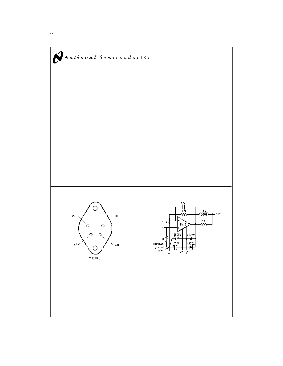
The LM12 is supplied in a four-lead, TO-3 package with V-
on the case. A gold-eutectic die-attach to a molybdenum in-
terface is used to avoid thermal fatigue problems. The LM12
is specified for either military or commercial temperature
range.
Connection Diagram
Typical Application
*
DS008704-1
4-pin glass epoxy TO-3
socket is available from
AUGAT INC.
Part number 8112-AG7
Bottom View
Order Number LM12CLK
See NS Package Number K04A
DS008704-2
*Low distortion (0.01%) audio amplifier
May 1999
LM12CL
80W
Operational
Amplifier
© 1999 National Semiconductor Corporation
DS008704
www.national.com

Absolute Maximum Ratings
(Note 1)
If Military/Aerospace specified devices are required,
please contact the National Semiconductor Sales Office/
Distributors for availability and specifications.
Total Supply Voltage (Note 1)
80V
Input Voltage
(Note 2)
Output Current
Internally Limited
Junction Temperature
(Note 3)
Storage Temperature Range
-65∞C to 150∞C
Lead Temperature
(Soldering, 10 seconds)
300∞C
Operating Ratings
Total Supply Voltage
15V to 60V
Case Temperature (Note 4)
0∞C to 70∞C
Electrical Characteristics
(Note 4)
Parameter
Conditions
Typ
25∞C
LM12CL
Units
Limits
Input Offset Voltage
±
10V
V
S
±
0.5 V
MAX
, V
CM
= 0
2
15/20
mV (max)
Input Bias Current
V- + 4V
V
CM
V+ -2V
0.15
0.7/1.0
µA (max)
Input Offset Current
V- +4V
V
CM
V+ -2V
0.03
0.2/0.3
µA (max)
Common Mode
V- +4V
V
CM
V+ -2V
86
70/65
dB (min)
Rejection
Power Supply
V+ = 0.5 V
MAX
,
90
70/65
dB (min)
Rejection
-6V
V-
-0.5 V
MAX
V- = -0.5 V
MAX
,
110
75/70
dB (min)
6V
V+
0.5 V
MAX
Output Saturation
t
ON
= 1 ms,
Threshold
V
IN
= 5 (10 ) mV,
I
OUT
= 1A
1.8
2.2/2.5
V (max)
8A
4
5/7
V (max)
10A
5
V (max)
Large Signal Voltage
t
ON
= 2 ms,
Gain
V
SAT
= 2V, I
OUT
= 0
100
30/20
V/mV (min)
V
SAT
= 8V, R
L
= 4
50
15/10
V/mV (min)
Thermal Gradient
P
DISS
= 50W, t
ON
= 65 ms
30
100
µV/W (max)
Feedback
Output-Current Limit
t
ON
= 10 ms, V
DISS
= 10V
13
16
A (max)
t
ON
= 100 ms, V
DISS
= 58V
1.5
0.9/0.6
A (min)
1.5
1.7
A (max)
Power Dissipation
t
ON
= 100 ms, V
DISS
= 20V
100
80/55
W (min)
Rating
V
DISS
= 58V
80
52/35
W (min)
DC Thermal Resistance
(Note 5) V
DISS
= 20V
2.3
2.9
∞C/W (max)
V
DISS
= 58V
2.7
4.5
∞C/W (max)
AC Thermal Resistance
(Note 5)
1.6
2.1
∞C/W (max)
Supply Current
V
OUT
= 0, I
OUT
= 0
60
120/140
mA (max)
Note 1: Absolute maximum ratings indicate limits beyond which damage to the device may occur. The maximum voltage for which the LM12 is guaranteed to operate
is given in the operating ratings and in Note 4. With inductive loads or output shorts, other restrictions described in applications section apply.
Note 2: Neither input should exceed the supply voltage by more than 50 volts nor should the voltage between one input and any other terminal exceed 60 volts.
Note 3: Operating junction temperature is internally limited near 225∞C within the power transistor and 160∞C for the control circuitry.
Note 4: The supply voltage is
±
30V (V
MAX
= 60V), unless otherwise specified. The voltage across the conducting output transistor (supply to output) is V
DISS
and
internal power dissipation is P
DISS
. Temperature range is 0∞C
T
C
70∞C where T
C
is the case temperature. Standard typeface indicates limits at 25∞C while bold-
face type refers to limits or special conditions over full temperature range. With no heat sink, the package will heat at a rate of 35∞C/sec per 100W of internal
dissipation.
Note 5: This thermal resistance is based upon a peak temperature of 200∞C in the center of the power transistor and a case temperature of 25∞C measured at the
center of the package bottom. The maximum junction temperature of the control circuitry can be estimated based upon a dc thermal resistance of 0.9∞C/W or an ac
thermal resistance of 0.6∞C/W for any operating voltage.
Although the output and supply leads are resistant to electrostatic discharges from handling, the input leads are not.
The part should be treated accordingly.
www.national.com
2

Output-Transistor Ratings (guaranteed)
Typical Performance Characteristics
Safe Area
DS008704-31
DC Thermal Resistance
DS008704-32
Pulse Thermal Resistance
DS008704-33
Pulse Power Limit
DS008704-34
Pulse Power Limit
DS008704-35
Peak Output Current
DS008704-36
Output Saturation Voltage
DS008704-37
Large Signal Response
DS008704-38
Follower Pulse Response
DS008704-39
Large Signal Gain
DS008704-40
Thermal Response
DS008704-41
Total Harmonic Distortion
DS008704-42
www.national.com
3
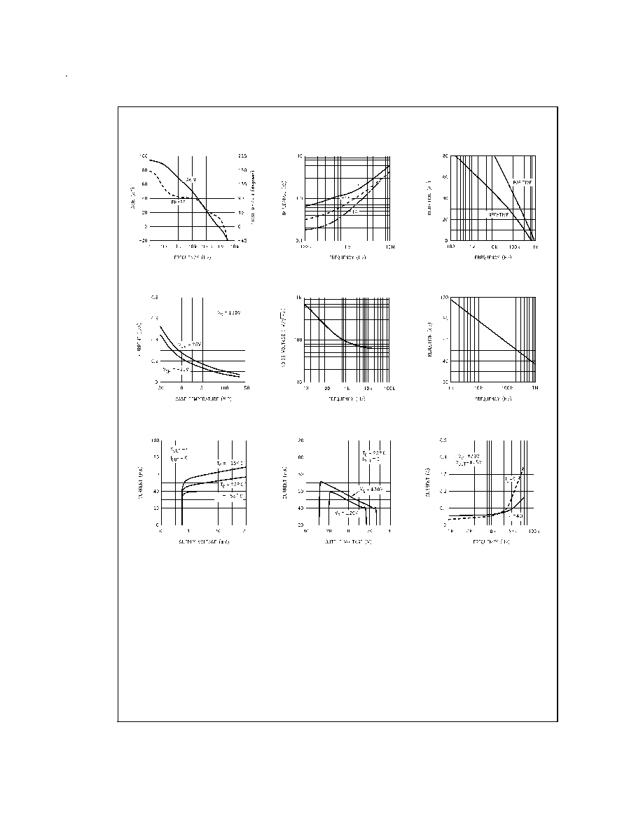
Typical Performance Characteristics
(Continued)
Application Information
GENERAL
Twenty five years ago the operational amplifier was a spe-
cialized design tool used primarily for analog computation.
However, the availability of low cost IC op amps in the late
1960's prompted their use in rather mundane applications,
replacing a few discrete components. Once a few basic prin-
ciples are mastered, op amps can be used to give exception-
ally good results in a wide range of applications while mini-
mizing both cost and design effort.
The availability of a monolithic power op amp now promises
to extend these advantages to high-power designs. Some
conventional applications are given here to illustrate op amp
design principles as they relate to power circuitry. The inevi-
table fall in prices, as the economies of volume production
are realized, will prompt their use in applications that might
now seem trivial. Replacing single power transistors with an
op amp will become economical because of improved per-
formance, simplification of attendant circuitry, vastly im-
proved fault protection, greater reliability and the reduction of
design time.
Power op amps introduce new factors into the design equa-
tion. With current transients above 10A, both the inductance
and resistance of wire interconnects become important in a
number of ways. Further, power ratings are a crucial factor in
determining performance. But the power capability of the IC
cannot be realized unless it is properly mounted to an ad-
equate heat sink. Thus, thermal design is of major impor-
tance with power op amps.
This application summary starts off by identifying the origin
of strange problems observed while using the LM12 in a
Frequency Response
DS008704-43
Output Impedance
DS008704-44
Power Supply Rejection
DS008704-45
Input Bias Current
DS008704-46
Input Noise Voltage
DS008704-47
Common Mode Rejection
DS008704-48
Supply Current
DS008704-49
Supply Current
DS008704-50
Cross-Supply Current
DS008704-51
www.national.com
4

Application Information
(Continued)
wide variety of designs with all sorts of fault conditions. A few
simple precautions will eliminate these problems. One
would do well to read the section on supply bypassing,
lead inductance, output clamp diodes, ground loops and
reactive loading before doing any experimentation.
Should there be problems with erratic operation,
blow-outs, excessive distortion or oscillation, another
look at these sections is in order.
The management and protection circuitry can also affect op-
eration. Should the total supply voltage exceed ratings or
drop below 15≠20V, the op amp shuts off completely. Case
temperatures above 150∞C also cause shut down until the
temperature drops to 145∞C. This may take several seconds,
depending on the thermal system. Activation of the dynamic
safe-area protection causes both the main feedback loop to
lose control and a reduction in output power, with possible
oscillations. In ac applications, the dynamic protection will
cause waveform distortion. Since the LM12 is well protected
against thermal overloads, the suggestions for determining
power dissipation and heat sink requirements are presented
last.
SUPPLY BYPASSING
All op amps should have their supply leads bypassed with
low-inductance capacitors having short leads and located
close to the package terminals to avoid spurious oscillation
problems. Power op amps require larger bypass capacitors.
The LM12 is stable with good-quality electrolytic bypass ca-
pacitors greater than 20 µF. Other considerations may re-
quire larger capacitors.
The current in the supply leads is a rectified component of
the load current. If adequate bypassing is not provided, this
distorted signal can be fed back into internal circuitry. Low
distortion at high frequencies requires that the supplies be
bypassed with 470 µF or more, at the package terminals.
LEAD INDUCTANCE
With ordinary op amps, lead-inductance problems are usu-
ally restricted to supply bypassing. Power op amps are also
sensitive to inductance in the output lead, particularly with
heavy capacitive loading. Feedback to the input should be
taken directly from the output terminal, minimizing common
inductance with the load. Sensing to a remote load must be
accompanied by a high-frequency feedback path directly
from the output terminal. Lead inductance can also cause
voltage surges on the supplies. With long leads to the power
source, energy stored in the lead inductance when the out-
put is shorted can be dumped back into the supply bypass
capacitors when the short is removed. The magnitude of this
transient is reduced by increasing the size of the bypass ca-
pacitor near the IC. With 20 µF local bypass, these voltage
surges are important only if the lead length exceeds a couple
feet (
>
1 µH lead inductance). Twisting together the supply
and ground leads minimizes the effect.
GROUND LOOPS
With fast, high-current circuitry, all sorts of problems can
arise from improper grounding. In general, difficulties can be
avoided by returning all grounds separately to a common
point. Sometimes this is impractical. When compromising,
special attention should be paid to the ground returns for the
supply bypasses, load and input signal. Ground planes also
help to provide proper grounding.
Many problems unrelated to system performance can be
traced to the grounding of line-operated test equipment used
for system checkout. Hidden paths are particularly difficult to
sort out when several pieces of test equipment are used but
can be minimized by using current probes or the new iso-
lated oscilloscope pre-amplifiers. Eliminating any direct
ground connection between the signal generator and the os-
cilloscope synchronization input solves one common prob-
lem.
OUTPUT CLAMP DIODES
When a push-pull amplifier goes into power limit while driv-
ing an inductive load, the stored energy in the load induc-
tance can drive the output outside the supplies. Although the
LM12 has internal clamp diodes that can handle several am-
peres for a few milliseconds, extreme conditions can cause
destruction of the IC. The internal clamp diodes are imper-
fect in that about half the clamp current flows into the supply
to which the output is clamped while the other half flows
across the supplies. Therefore, the use of external diodes to
clamp the output to the power supplies is strongly recom-
mended. This is particularly important with higher supply
voltages.
Experience has demonstrated that hard-wire shorting the
output to the supplies can induce random failures if these ex-
ternal clamp diodes are not used and the supply voltages are
above
±
20V. Therefore it is prudent to use outputclamp di-
odes even when the load is not particularly inductive. This
also applies to experimental setups in that blowouts have
been observed when diodes were not used. In packaged
equipment, it may be possible to eliminate these diodes, pro-
viding that fault conditions can be controlled.
Heat sinking of the clamp diodes is usually unimportant in
that they only clamp current transients. Forward drop with
15A fault transients is of greater concern. Usually, these
transients die out rapidly. The clamp to the negative supply
can have somewhat reduced effectiveness under worst case
conditions should the forward drop exceed 1.0V. Mounting
this diode to the power op amp heat sink improves the situ-
ation. Although the need has only been demonstrated with
some motor loads, including a third diode (D3 above) will
eliminate any concern about the clamp diodes. This diode,
however, must be capable of dissipating continuous power
as determined by the negative supply current of the op amp.
REACTIVE LOADING
The LM12 is normally stable with resistive, inductive or
smaller capacitive loads. Larger capacitive loads interact
with the open-loop output resistance (about 1
) to reduce
the phase margin of the feedback loop, ultimately causing
oscillation. The critical capacitance depends upon the feed-
back applied around the amplifier; a unity-gain follower can
handle about 0.01 µF, while more than 1 µF does not cause
problems if the loop gain is ten. With loop gains greater than
unity, a speedup capacitor across the feedback resistor will
DS008704-6
www.national.com
5