
LM12L458
12-Bit + Sign Data Acquisition System with
Self-Calibration
General Description
The LM12L458 is a highly integrated 3.3V Data Acquisition
System. It combines a fully-differential self-calibrating (cor-
recting linearity and zero errors) 13-bit (12-bit + sign)
analog-to-digital converter (ADC) and sample-and-hold
(S/H) with extensive analog functions and digital functional-
ity. Up to 32 consecutive conversions, using two's comple-
ment format, can be stored in an internal 32-word (16-bit
wide) FIFO data buffer. An internal 8-word RAM can store
the conversion sequence for up to eight acquisitions through
the LM12L458's eight-input multiplexer. The LM12L458 can
also operate with 8-bit + sign resolution and in a supervisory
"watchdog" mode that compares an input signal against two
programmable limits. Programmable acquisition times and
conversion rates are possible through the use of internal
clock-driven timers.
All registers, RAM, and FIFO are directly addressable
through the high speed microprocessor interface to either an
8-bit or 16-bit databus. The LM12L458 includes a direct
memory access (DMA) interface for high-speed conversion
data transfer.
Applications
n
Data Logging
n
Process Control
n
Energy Management
n
Medical Instrumentation
Key Specifications
(f
CLK
= 6 MHz)
n
Resolution
12-bit + sign or 8-bit + sign
n
13-bit conversion time
7.3 µs
n
9-bit conversion time
3.5 µs
n
13-bit Through-put rate
106k samples/s (min)
n
Comparison time ("watchdog" mode)
1.8 µs (max)
n
ILE
±
1 LSB (max)
n
V
IN
range
GND to V
A
+
n
Power dissipation
15 mW (max)
n
Stand-by mode
5 µW (typ)
n
Single supply
3V to 5.5V
Features
n
Three operating modes: 12-bit + sign, 8-bit + sign, and
"watchdog"
n
Single-ended or differential inputs
n
Built-in Sample-and-Hold
n
Instruction RAM and event sequencer
n
8-channel multiplexer
n
32-word conversion FIFO
n
Programmable acquisition times and conversion rates
n
Self-calibration and diagnostic mode
n
8- or 16-bit wide databus microprocessor or DSP
interface
n
CMOS compatible I/O
TRI-STATE
Æ
is a registered trademark of National Semiconductor Corporation.
AT
Æ
is a registered trademark of International Business Machines Corporation.
July 1999
LM12L458
12-Bit
+
Sign
Data
Acquisition
System
with
Self-Calibration
© 1999 National Semiconductor Corporation
DS011711
www.national.com
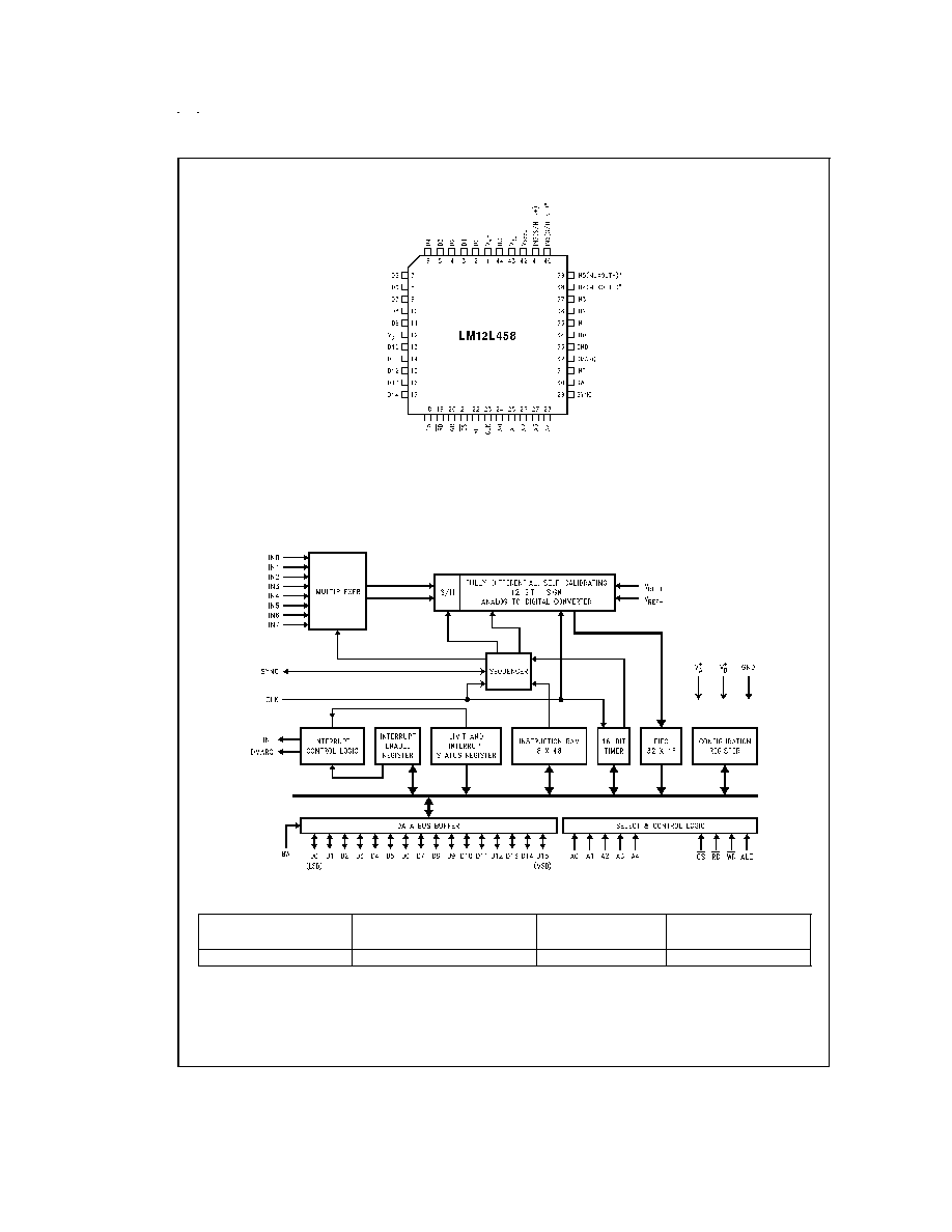
Connection Diagram
Functional Diagram
Ordering Information
Guaranteed
Guaranteed
Order
See NS
Clock Freq (min)
Linearity Error (max)
Part Number
Package Number
6 MHz
±
1.0 LSB
LM12L458CIV
V44A
DS011711-1
*
Pin names in ( ) apply to the LM12L454.
Order Number LM12L458CIV
See NS Package Number V44A
LM12L458
DS011711-3
www.national.com
2

Absolute Maximum Ratings
(Notes 1, 2)
If Military/Aerospace specified devices are required,
please contact the National Semiconductor Sales Office/
Distributors for availability and specifications.
Supply Voltage (V
A
+ and V
D
+)
6.0V
Voltage at Input and Output Pins
except IN0≠IN7 (LM12L458)
-0.3V to V
+
+ 0.3V
Voltage at Analog Inputs
IN0≠IN7 (LM12L458)
GND - 5V to V
+
+ 5V
|V
A
+ - V
D
+|
300 mV
Input Current at Any Pin (Note 3)
±
5 mA
Package Input Current (Note 3)
±
20 mA
Power Dissipation (T
A
= 25∞C)
V Package (Note 4)
875 mW
Storage Temperature
-65∞C to +150∞C
Lead Temperature
V Package, Infrared, 15 sec.
+300∞C
ESD Susceptibility (Note 5)
1.5 kV
See AN-450 "Surface Mounting Methods and Their Effect
on Product Reliability" for other methods of soldering
surface mount devices.
Operating Ratings
(Notes 1, 2)
Temperature Range
(T
min
T
A
T
max
)
LM12L458CIV
-40∞C
T
A
85∞C
Supply Voltage
V
A
+, V
D
+
3.0V to 5.5V
|V
A
+ - V
D
+|
100 mV
V
IN+
Input Range
GND
V
IN+
V
A
+
V
IN-
Input Range
GND
V
IN-
V
A
+
V
REF+
Input Voltage
1V
V
REF+
V
A
+
V
REF-
Input Voltage
0V
V
REF-
V
REF+
- 1V
V
REF+
- V
REF-
1V
V
REF
V
A
+
V
REF
Common Mode
Range (Note 16)
0.1 V
A
+
V
REFCM
0.6 V
A
+
Converter Characteristics
The following specifications apply for V
A
+ = V
D
+ = 3.3V, V
REF+
= 2.5V, V
REF-
= 0V, 12-bit + sign conversion mode, f
CLK
=
6.0 MHz, R
S
= 25
, source impedance for V
REF+
and V
REF-
25
, fully-differential input with fixed 1.25V common-mode volt-
age, and minimum acquisition time unless otherwise specified. Boldface limits apply for T
A
= T
J
= T
MIN
to T
MAX
; all other
limits T
A
= T
J
= 25∞C. (Notes 6, 7, 8, 9)
Symbol
Parameter
Conditions
Typical
Limits
Unit
(Note 10)
(Note 11)
(Limit)
ILE
Positive and Negative Integral
Linearity Error
After Auto-Cal (Notes 12, 17)
±
1/2
±
1
LSB (max)
TUE
Total Unadjusted Error
After Auto-Cal (Note 12)
±
1
LSB
Resolution with No Missing Codes
After Auto-Cal (Note 12)
13
Bits (max)
DNL
Differential Non-Linearity
After Auto-Cal
±
1
LSB (max)
Zero Error
After Auto-Cal (Notes 13, 17)
±
1/4
±
1
LSB (max)
Positive Full-Scale Error
After Auto-Cal (Notes 12, 17)
±
1/2
±
3
LSB (max)
Negative Full-Scale Error
After Auto-Cal (Notes 12, 17)
±
1/2
±
3
LSB (max)
DC Common Mode Error
(Note 14)
±
2
±
4
LSB (max)
ILE
8-Bit + Sign and "Watchdog" Mode
Positive and Negative Integral
Linearity Error
(Note 12)
±
1/2
LSB (max)
TUE
8-Bit + Sign and "Watchdog" Mode
Total Unadjusted Error
After Auto-Zero
±
1/2
±
3/4
LSB (max)
8-Bit + Sign and "Watchdog" Mode
Resolution with No Missing Codes
9
Bits (max)
DNL
8-Bit + Sign and "Watchdog" Mode
Differential Non-Linearity
±
1
LSB (max)
8-Bit + Sign and "Watchdog" Mode
Zero Error
After Auto-Zero
±
1/2
LSB (max)
8-Bit + Sign and "Watchdog" Positive
and Negative Full-Scale Error
±
1/2
LSB (max)
8-Bit + Sign and "Watchdog" Mode DC
Common Mode Error
±
1/8
LSB
Multiplexer Channel-to-Channel
Matching
±
0.05
LSB
V
IN+
Non-Inverting Input Range
GND
V (min)
V
A
+
V (max)
www.national.com
3

Converter Characteristics
(Continued)
The following specifications apply for V
A
+ = V
D
+ = 3.3V, V
REF+
= 2.5V, V
REF-
= 0V, 12-bit + sign conversion mode, f
CLK
=
6.0 MHz, R
S
= 25
, source impedance for V
REF+
and V
REF-
25
, fully-differential input with fixed 1.25V common-mode volt-
age, and minimum acquisition time unless otherwise specified. Boldface limits apply for T
A
= T
J
= T
MIN
to T
MAX
; all other
limits T
A
= T
J
= 25∞C. (Notes 6, 7, 8, 9)
Symbol
Parameter
Conditions
Typical
Limits
Unit
(Note 10)
(Note 11)
(Limit)
V
IN-
Inverting Input Range
GND
V (min)
V
A
+
V (max)
V
IN+
- V
IN-
Differential Input Voltage Range
-V
A
+
V (min)
V
A
+
V (max)
Common Mode Input Voltage Range
GND
V (min)
V
A
+
V (max)
PSS
Power Supply
Zero Error
V
A
+ = V
D
+ = 3.3V
±
10%
±
0.2
±
1.75
LSB (max)
Sensitivity
Full-Scale Error
V
REF+
= 2.5V, V
REF-
= GND
±
0.4
±
2
LSB (max)
(Note 15)
Linearity Error
±
0.2
LSB
C
REF
V
REF+
/V
REF-
Input Capacitance
85
pF
C
IN
Selected Multiplexer Channel Input
75
pF
Capacitance
Converter AC Characteristics
The following specifications apply for V
A
+ = V
D
+ = 3.3V, V
REF+
= 2.5V, V
REF-
= 0V, 12-bit + sign conversion mode, f
CLK
= 6.0
MHz, R
S
= 25
, source impedance for V
REF+
and V
REF-
25
, fully-differential input with fixed 1.25V common-mode voltage,
and minimum acquisition time unless otherwise specified. Boldface limits apply for T
A
= T
J
= T
MIN
to T
MAX
; all other limits
T
A
= T
J
= 25∞C. (Notes 6, 7, 8, 9)
Symbol
Parameter
Conditions
Typical
Limits
Unit
(Note 10)
(Note 11)
(Limit)
Clock Duty Cycle
50
%
40
% (min)
60
% (max)
t
C
Conversion Time
13-Bit Resolution,
44 (t
CLK
)
44 (t
CLK
) + 50 ns
(max)
Sequencer State S5 (
Figure 15)
9-Bit Resolution,
21 (t
CLK
)
21 (t
CLK
) + 50 ns
(max)
Sequencer State S5 (
Figure 15)
t
A
Acquisition Time
Sequencer State S7 (
Figure 15)
9 (t
CLK
)
9 (t
CLK
) + 50 ns
(max)
Built-in minimum for 13-Bits
Built-in minimum for 9-Bits and
2 (t
CLK
)
2 (t
CLK
) + 50 ns
(max)
"Watchdog" mode
t
Z
Auto-Zero Time
Sequencer State S2 (
Figure 15)
76 (t
CLK
)
76 (t
CLK
) + 50 ns
(max)
t
CAL
Full Calibration Time
Sequencer State S2 (
Figure 15)
4944 (t
CLK
)
4944 (t
CLK
) + 50 ns
(max)
Throughput Rate
107
106
kHz
(Note 18)
(min)
t
WD
"Watchdog" Mode
Sequencer States S6, S4,
11 (t
CLK
)
11 (t
CLK
) + 50 ns
(max)
Comparison Time
and S5 (
Figure 15)
t
PU
Power-Up Time
10
ms
t
WU
Wake-Up Time
10
ms
www.national.com
4

DC Characteristics
The following specifications apply for V
A
+ = V
D
+ = 3.3V, V
REF+
= 2.5V, V
REF-
= 0V, f
CLK
= 6.0 MHz and minimum acquisition
time unless otherwise specified. Boldface limits apply for T
A
= T
J
= T
MIN
to T
MAX
; all other limits T
A
= T
J
= 25∞C. (Notes 6,
7, 8)
Symbol
Parameter
Conditions
Typical
Limits
Unit
(Note 10)
(Note 11)
(Limit)
I
D
+
V
D
+ Supply Current
CS = "1"
0.4
1.0
mA (max)
I
A
+
V
A
+ Supply Current
CS = "1"
2.25
3.5
mA (max)
I
ST
Stand-By Supply Current
Power-Down Mode Selected
(I
D
+ + I
A
+)
Clock Stopped
1.5
4.5
µA (max)
6 MHz Clock
30
µA (max)
Multiplexer ON-Channel
Leakage Current
V
A
+ = 3.6V
ON-Channel = 3.6V
OFF-Channel = 0V
0.1
0.3
µA (max)
ON-Channel = 0V
OFF-Channel = 3.6V
0.1
0.3
µA (max)
Multiplexer OFF-Channel
Leakage Current
V
A
+ = 3.6V
ON-Channel = 3.6V
OFF-Channel = 0V
0.1
0.3
µA (max)
ON-Channel = 0V
OFF-Channel = 3.6V
0.1
0.3
µA (max)
R
ON
Multiplexer ON-Resistance
V
IN
= 3.3V
850
1500
V
IN
= 1.65V
1300
2000
V
IN
= 0V
830
1500
Multiplexer
Channel-to-Channel
R
ON
matching
V
IN
= 3.3V
±
1.0%
±
3.0%
V
IN
= 1.65V
±
1.0%
±
3.0%
V
IN
= 0V
±
1.0%
±
3.0%
Digital Characteristics
The following specifications apply for V
A
+ = V
D
+ = 3.3V, unless otherwise specified. Boldface limits apply for T
A
= T
J
=
T
MIN
to T
MAX
; all other limits T
A
= T
J
= 25∞C. (Notes 6, 7, 8)
Symbol
Parameter
Conditions
Typical
Limits
Unit
(Note 10)
(Note 11)
(Limit)
V
IN(1)
Logical "1" Input Voltage
V
A
+ = V
D
+ = 3.6V
2.0
V (min)
V
IN(0)
Logical "0" Input Voltage
V
A
+ = V
D
+ = 3.0V
0.7
V (max)
ALE, Pin 22
0.6
I
IN(1)
Logical "1" Input Current
V
IN
= 3.3V
0.005
1.0
µA (max)
2.0
I
IN(0)
Logical "0" Input Current
V
IN
= 0V
-0.005
-1.0
µA (max)
-2.0
C
IN
D0≠D15 Input Capacitance
6
pF
V
OUT(1)
Logical "1" Output Voltage
V
A
+ = V
D
+ = 3.0V
I
OUT
= -360 µA
2.4
V (min)
I
OUT
= -10 µA
2.85
V (min)
V
OUT(0)
Logical "0" Output Voltage
V
A
+ = V
D
+ = 3.0V
I
OUT
= 1.6 mA
0.4
V (max)
I
OUT
= 10 µA
0.1
I
OUT
TRI-STATE
Æ
Output Leakage Current
V
OUT
= 0V
-0.01
-3.0
µA (max)
V
OUT
= 3.3V
0.01
3.0
µA (max)
www.national.com
5