 | –≠–ª–µ–∫—Ç—Ä–æ–Ω–Ω—ã–π –∫–æ–º–ø–æ–Ω–µ–Ω—Ç: LM148JAN | –°–∫–∞—á–∞—Ç—å:  PDF PDF  ZIP ZIP |
LM148JAN
Quad 741 Op Amps
General Description
The LM148 is a true quad LM741. It consists of four inde-
pendent, high gain, internally compensated, low power op-
erational amplifiers which have been designed to provide
functional characteristics identical to those of the familiar
LM741 operational amplifier. In addition the total supply
current for all four amplifiers is comparable to the supply
current of a single LM741 type op amp. Other features
include input offset currents and input bias current which are
much less than those of a standard LM741. Also, excellent
isolation between amplifiers has been achieved by indepen-
dently biasing each amplifier and using layout techniques
which minimize thermal coupling.
The LM148 can be used anywhere multiple LM741 or
LM1558 type amplifiers are being used and in applications
where amplifier matching or high packing density is required.
Features
n
741 op amp operating characteristics
n
Class AB output stage -- no crossover distortion
n
Pin compatible with the LM124
n
Overload protection for inputs and outputs
n
Low supply current drain:
0.6 mA/Amplifier
n
Low input offset voltage:
1 mV
n
Low input offset current:
4 nA
n
Low input bias current
30 nA
n
High degree of isolation between amplifiers:
120 dB
n
Gain bandwidth product (unity gain):
1.0 MHz
Ordering Information
NS PART NUMBER
SMD PART NUMBER
NS PACKAGE NUMBER
PACKAGE DESCRIPTION
JL148BCA
JM38510/11001BCA
J14A
14LD CERDIP
JL148BDA
JM38510/11001BDA
W14B
14LD CERPACK
JL148BZA
JM38510/11001BZA
WG14A
14LD Ceramic SOIC
JL148SCA
JM38510/11001SCA
J14A
14LD CERDIP
JL148SDA
JM38510/11001SDA
W14B
14LD CERPACK
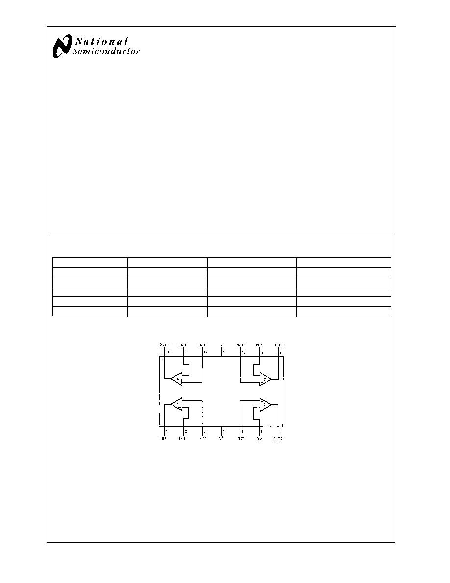
Connection Diagram
20122702
Top View
See NS Package Number J14A, W14B, WG14A
February 2005
LM148JAN
Quad
741
Op
Amp
© 2005 National Semiconductor Corporation
DS201227
www.national.com
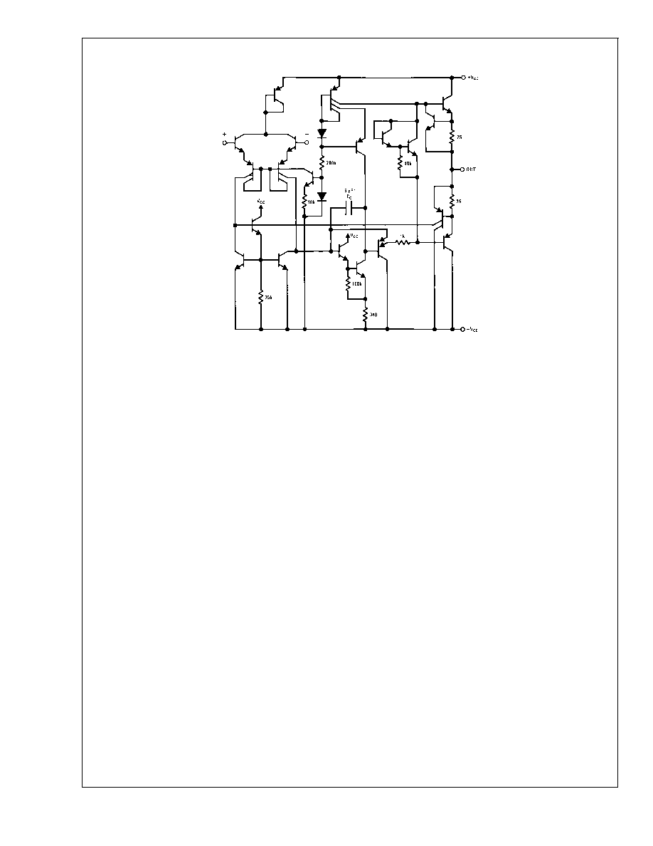
Schematic Diagram
20122701
* 1 pF in the LM149
LM148JAN
www.national.com
2
Absolute Maximum Ratings
(Note 1)
Supply Voltage
±
22V
Input Voltage Range
±
20V
Input Current Range
-0.1mA to 10mA
Differential Input Voltage (Note 2)
±
30V
Output Short Circuit Duration (Note 3)
Continuous
Power Dissipation (P
d
at 25∞C) (Note 4)
CERDIP
CERPACK
400mW
350mW
Thermal Resistance
JA
CERDIP (Still Air)
CERDIP (500LF/ Min Air flow)
CERPACK (Still Air)
CERPACK (500LF/ Min Air flow)
Ceramic SOIC (Still Air)
Ceramic SOIC (500LF/ Min Air flow)
103∞C/W
52∞C/W
140∞C/W
100∞C/W
176∞C/W
116∞C/W
JC
CERDIP
CERPACK
Ceramic SOIC
19∞C/W
25∞C/W
25∞C/W
Package Weight (typical)
CERDIP
CERPACK
Ceramic SOIC
TBD
465mg
415mg
Maximum Junction Temperature (T
JMAX
)
175∞C
Operating Temperature Range
-55∞C
T
A
+125∞C
Storage Temperature Range
-65∞C
T
A
+150∞C
Lead Temperature (Soldering, 10 sec.) Ceramic
300∞C
ESD tolerance (Note 5)
500V
Quality Conformance Inspection
MIL-STD-883, Method 5005 -- Group A
Subgroup
Description
Temp ( ∞C)
1
Static tests at
+25
2
Static tests at
+125
3
Static tests at
-55
4
Dynamic tests at
+25
5
Dynamic tests at
+125
6
Dynamic tests at
-55
7
Functional tests at
+25
8A
Functional tests at
+125
8B
Functional tests at
-55
9
Switching tests at
+25
10
Switching tests at
+125
11
Switching tests at
-55
LM148JAN
www.national.com
3

Electrical Characteristics
DC PARAMETERS (The following conditions apply to all parameters, unless otherwise specified.)
±
V
CC
=
±
20V, V
CM
= 0V,
measure each amplifier.
Symbol
Parameter
Conditions
Notes
Min Max
Units
Sub-
groups
V
IO
Input Offset Voltage
+V
CC
= 35V, -V
CC
= -5V,
V
CM
= -15V
-5.0 +5.0
mV
1
-6.0 +6.0
mV
2, 3
+V
CC
= 5V, -V
CC
= -35V,
V
CM
= +15V
-5.0 +5.0
mV
1
-6.0 +6.0
mV
2, 3
-5.0 +5.0
mV
1
-6.0 +6.0
mV
2, 3
+V
CC
= 5V, -V
CC
= -5V,
-5.0 +5.0
mV
1
-6.0 +6.0
mV
2, 3
Delta V
IO
/
Delta
T
Input Offset Voltage
Temperature Stability
25∞C
T
A
125∞C
(Note 6)
-25
25
µV/∞C
2
-55∞C
T
A
25∞C
(Note 6)
-25
25
µV/∞C
3
I
IO
Input Offset Current
+V
CC
= 35V, -V
CC
= -5V,
V
CM
= -15V
-25
+25
nA
1, 2
-75
+75
nA
3
+V
CC
= 5V, -V
CC
= -35V,
V
CM
= +15V
-25
+25
nA
1, 2
-75
+75
nA
3
-25
+25
nA
1, 2
-75
+75
nA
3
+V
CC
= 5V, -V
CC
= -5V,
-25
+25
nA
1, 2
-75
+75
nA
3
Delta I
IO
/
Delta
T
Input Offset Current
Temperature Stability
25∞C
T
A
125∞C
(Note 6)
-200 200
pA/∞C
2
-55∞C
T
A
25∞C
(Note 6)
≠400 400
pA/∞C
3
±
I
IB
Input Bias Current
+V
CC
= 35V, -V
CC
= -5V,
V
CM
= -15V
-0.1 100
nA
1, 2
-0.1 325
nA
3
+V
CC
= 5V, -V
CC
= -35V,
V
CM
= +15V
-0.1 100
nA
1, 2
-0.1 325
nA
3
-0.1 100
nA
1, 2
-0.1 325
nA
3
+V
CC
= 5V, -V
CC
= -5V,
-0.1 100
nA
1, 2
-0.1 325
nA
3
PSRR+
Power Supply Rejection Ratio
-V
CC
= -20V, +V
CC
= 20V to 10V
(Note 7)
-100 100
µV/V
1, 2, 3
PSRR-
Power Supply Rejection Ratio
+V
CC
= 20V, -V
CC
= -20V to -10V (Note 7)
-100 100
µV/V
1, 2, 3
CMRR
Common Mode Rejection Ratio V
CM
=
±
15 V,
±
5V
V
CC
±
35V
76
dB
1, 2, 3
Electrical Characteristics
AC / DC PARAMETERS (The following conditions apply to all parameters, unless otherwise specified.)
±
V
CC
=
±
20V, V
CM
= 0V, measure each amplifier.
Symbol
Parameter
Conditions
Notes
Min Max
Units
Sub-
groups
+ I
OS
Short Circuit Current
+V
CC
= 15V, -V
CC
= -15V,
V
CM
= -10V
-55
mA
1, 2
-75
mA
3
- I
OS
Short Circuit Current
+V
CC
= 15V, -V
CC
= -15V,
V
CM
= +10V
55
mA
1, 2
75
mA
3
I
CC
Power Supply Current
+V
CC
= 15V, -V
CC
= -15V
3.6
mA
1
4.5
mA
2, 3
-A
VS
Open Loop Voltage Gain
V
OUT
= -15V, R
L
= 10K
50
V/mV
4
25
V/mV
5, 6
V
OUT
= -15V, R
L
= 2K
50
V/mV
4
25
V/mV
5, 6
LM148JAN
www.national.com
4

Electrical Characteristics
(Continued)
AC / DC PARAMETERS (The following conditions apply to all parameters, unless otherwise specified.)
±
V
CC
=
±
20V, V
CM
= 0V, measure each amplifier.
Symbol
Parameter
Conditions
Notes
Min Max
Units
Sub-
groups
+A
VS
Open Loop Voltage Gain
V
OUT
= +15V, R
L
= 10K
50
V/mV
4
25
V/mV
5, 6
V
OUT
= +15V, R
L
= 2K
50
V/mV
4
25
V/mV
5, 6
A
VS
Open Loop Voltage Gain
V
CC
=
±
5V, V
OUT
=
±
2V, R
L
=
10K
10
V/mV
4, 5, 6
V
CC
=
±
5V, V
OUT
=
±
2V, R
L
= 2K
10
V/mV
4, 5, 6
+V
OP
Output Voltage Swing
R
L
= 10K
+16
V
4, 5, 6
R
L
= 2K
+15
V
4, 5, 6
-V
OP
Output Voltage Swing
R
L
= 10K
-16
V
4, 5, 6
R
L
= 2K
-15
V
4, 5, 6
TR
TR
Transient Response Time
V
IN
= 50mV, A
V
= 1
1
µS
7, 8A, 8B
TR
OS
Transient Response Time
V
IN
= 50mV, A
V
= 1
25
%
7, 8A, 8B
±
SR
Slew Rate
V
IN
= -5V to +5V, A
V
= 1
0.2
V/µS
7, 8A, 8B
V
IN
= +5V to -5V, A
V
= 1
0.2
V/µS
7, 8A, 8B
Electrical Characteristics
AC PARAMETERS (The following conditions apply to all parameters, unless otherwise specified.)
±
V
CC
=
±
20V, V
CM
= 0V,
measure each amplifier.
Symbol
Parameter
Conditions
Notes
Min Max
Units
Sub-
groups
NI
BB
Noise (Broadband)
BW = 10Hz to 5KHz
15
µV
RMS
7
NI
PC
Noise (Popcorn)
R
S
= 20K
40
µV
PK
7
C
S
Channel Separation
V
IN
=
±
10V, A to B, R
L
= 2K
80
dB
7
V
IN
=
±
10V, A to C, R
L
= 2K
80
dB
7
V
IN
=
±
10V, A to D, R
L
= 2K
80
dB
7
V
IN
=
±
10V, B to A, R
L
= 2K
80
dB
7
V
IN
=
±
10V, B to C, R
L
= 2K
80
dB
7
V
IN
=
±
10V, B to D, R
L
= 2K
80
dB
7
V
IN
=
±
10V, C to A, R
L
= 2K
80
dB
7
V
IN
=
±
10V, C to B, R
L
= 2K
80
dB
7
V
IN
=
±
10V, C to D, R
L
= 2K
80
dB
7
V
IN
=
±
10V, D to A, R
L
= 2K
80
dB
7
V
IN
=
±
10V, D to B, R
L
= 2K
80
dB
7
V
IN
=
±
10V, D to C, R
L
= 2K
80
dB
7
Electrical Characteristics
DC DRIFT PARAMETERS (The following conditions apply to all parameters, unless otherwise specified.)
±
V
CC
=
±
20V, V
CM
=
0V, measure each amplifier. Delta calculations performed on JAN S and QMLV devices at group B, subgroup 5 only.
Symbol
Parameter
Conditions
Notes
Min Max
Units
Sub-
groups
V
IO
Input Offset Voltage
-1
1
mV
1
±
I
IB
Input Bias Current
-15
15
nA
1
LM148JAN
www.national.com
5