LM1572
1.5A, 500kHz Step-down Voltage Regulator
General Description
The LM1572 is a 500kHz step-down (buck) switching volt-
age regulator capable of driving up to 1.5A in to a load while
occupying a very small PCB area. Current Mode Control
results in superior transient response and regulation over a
wider range of operating conditions. National's advanced
analog bipolar, CMOS plus DMOS process enables high
efficiency at high switching frequency, and the internal
150m
MOSFET switch provides more power from a
smaller package.
The LM1572 has programmable soft-start and frequency
foldback to limit the inrush current, and a TTL compatible
shutdown for easy sequencing. It draws 2.3mA of supply
current in standby mode, and only 26µA in shutdown mode.
The LM1572 is available in a TSSOP-16 package with an
adjustable output or fixed outputs of 5V and 3.3V. The ad-
justable version can be set between 2.42V and 5V.
Features
n
500kHz clock allows small, surface mount components
n
150m
MOSFET switch
n
Guaranteed load current of 1.5A
n
Current mode control
n
Programmable soft-start
n
Internally set slope compensation
n
TTL compatible shutdown
n
Fixed 5V, 3.3V or adjustable output
n
Low shutdown supply current of 26µA
n
Cycle-by-cycle current limit
n
Short-circuit protection and thermal protection
n
TSSOP-16 package
Applications
n
LCD Monitors and TVs
n
Set-Top Boxes
n
Cable Modems
n
Down conversion from 12V in local/distributed systems
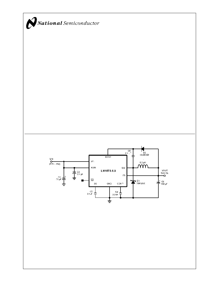
Typical Applications (Fixed/Adjustable Voltage Parts)
20033313
July 2002
LM1572
1.5A,
500kHz
Step-down
V
oltage
Regulator
© 2002 National Semiconductor Corporation
DS200333
www.national.com

Typical Applications (Fixed/Adjustable Voltage Parts)
(Continued)
20033314
Connection Diagram
20033315
16-Lead TSSOP
NS Package Number MTC16
Pin Description
BOOT (Pin 1) - Bootstrap pin. It provides the upper rail for
the floating driver stage of the internal MOSFET switch, the
lower rail being the switching node (Pins 5 and 6). A small
decoupling capacitor (typically 0.1µF-0.22µF) is therefore
connected between the Bootstrap pin and the switching
node. This capacitor should be 0.18µF-0.22µF for applica-
tions with an output voltage greater than 3.3V, if the mini-
mum load (including the current drawn by internal/external
feedback resistor divider) is less than 1mA. Additional drive
voltage is provided by connecting this pin directly to the 5V
output rail via a diode as shown in the Typical Application
Circuit for the fixed voltage part. The same method can be
used for an adjustable part provided the part is adjusted for
an output of 5V. For other output voltages (between 2.42V to
5V) a more general method of providing this external drive
voltage is illustrated in the Typical Application Circuit for the
adjustable part. Note that the NPN signal transistor shown,
must have a guaranteed hfe greater than 400. Damage can
occur to Pin 1 if it is connected (via a diode) to any external
voltage source greater than 6V.
AV
IN
(Pin 2) - This is the Analog V
IN
and provides the supply
to the internal control circuitry, the (Power) V
IN
pins (Pins
3,4) providing the supply to the internal power stage. In the
simplest layout scheme, the Analog V
IN
pin can simply be
connected to the V
IN
pins directly on the pads where the IC
is mounted. But for better noise rejection the trace to Pin 2
can be routed separately from the (Power) V
IN
trace, starting
from the positive terminal of the input capacitor. A simple RC
filter solution can also be used for better results, particularly
at low input voltages. This consists of a 10
resistor con-
nected between Analog V
IN
and V
IN
, and a 0.47µF capacitor
between Analog V
IN
and Ground. Note that if this RC filter is
used, a 1M
resistor between Pin 1 and Ground is also
required.
LM1572
www.national.com
2

Pin Description
(Continued)
V
IN
(Pins 3,4) - This is the input supply to the power stage
(connected to the Drain of the switching MOSFET). To aid
thermal dissipation from the die, two pins are used for this
function. Both these pins must be connected together, very
close to the IC, onto a large PCB copper plane.
SW (Pins 5,6) - This is the Source of the internal switching
MOSFET and forms the 'switching node' of the buck con-
verter. These two pins should be connected together on the
PCB close to the IC. The length of the trace from this node to
the cathode of the catch diode, and from the anode of the
diode to the IC ground must be kept very small. The maxi-
mum inductance connected to the switching node (for any
application) is recommended to be 15µH. See the Inductor
Selection procedure for more details.
GND (Pins 7,9,13,14) - This is the Ground for the IC and for
the input and output rails of the buck converter. To aid
thermal dissipation from the die, four pins are used for this
function. Connect as many as possible of these ground pins
together, close to the IC onto a large PCB copper plane. A
two-sided PCB with one side serving as a 'ground plane' is
strongly recommended. The ground pins must then connect
to the ground plane very close to the IC through several vias.
The vias also serve to transfer heat to the other side of the
board for better thermal management.
SD (Pin 8) - Shutdown/Standby/UVLO Pin. This pin actually
has two thresholds. If it is taken below 2.38V (typical), the
switch turns off and the output of the converter falls to
zero.This is the 'standby mode'. The internal circuitry of the
IC remains active, continuing to draw about 2.3mA from the
input. If the voltage on this pin is lowered below 1V (typical),
the IC enters 'shutdown mode' drawing only 26 µA from the
input. Above 2.38V, the switching action resumes, and so
this pin can also be used to set an undervoltage lockout
threshold (UVLO) for the input rail. If this pin is not intended
to be used actively, it can be left floating to allow continuous
switching. The voltage on this pin should not exceed 7V to
avoid damage.
NC (Pins 10,11) - No Internal Connection.
SS (Pin 12) - Softstart pin. A small capacitor connected from
this pin to ground programs the amount of softstart. This
capacitor charges up by means of an internal 4.5µA current
source, during power-up, and also whenever the output of
the converter is enabled. The allowed duty cycle increases
slowly as the capacitor charges, reaching the maximum
allowed when the voltage on this pin approaches 2V. The
capacitor continues to charge, finally reaching 6V, at which
level it is internally clamped. This pin is internally forced to
ground (to discharge the softstart capacitor and to reset the
softstart function) whenever the shutdown pin is taken below
2.38V. If the softstart feature is not required, the softstart pin
can be left floating.
FB (Pin 15) - This is the feedback pin for the IC and is used
to set the output of the converter to regulate to the desired
value. For the fixed voltage part this pin is normally con-
nected directly to the output. For the adjustable part, a
resistive divider is used between the output and ground, so
that the voltage on this pin is 2.42V when the output is at the
required level. For fixed voltage parts, the internal divider
draws about 0.5mA, a consideration possibly affecting the
choice of the bootstrap capacitor (see description of Pin 1
above).
COMP (Pin 16) - This is the output of the error transconduc-
tance amplifier and is used for frequency compensation of
the feedback loop. A small capacitor from this pin to ground
(about 3.3nF to 6.8nF) provides the simplest loop compen-
sation, but a series resistor-capacitor combination (R be-
tween 1k to 1.5k) may also be used to improve the phase
margin/crossover frequency of the loop. The voltage on this
pin is at about 1V at very light loads. Under very heavy loads
or under output short-circuit, the voltage on this pin clamps
to 2V, and the converter enters protective foldback. The IC
automatically recovers from this mode when the load is
reduced.
LM1572
www.national.com
3
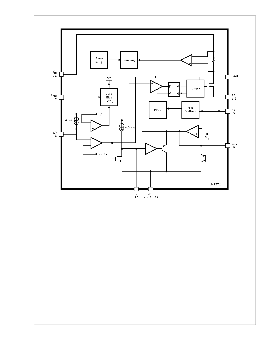
Block Diagram
20033312
LM1572
www.national.com
4

Absolute Maximum Ratings
(Note 1)
If Military/Aerospace specified devices are required,
please contact the National Semiconductor Sales Office/
Distributors for availability and specifications.
ESD Tolerance (Note 2)
2kV
Input Voltage
17V
SD Pin Voltage
7V
FB Pin Voltage (All Options)
7V
Storage Temp. Range
-65∞C to 150∞C
Junction Temperature
150∞C
Operating Ratings
Supply Voltage (V
IN
) (Note 3)
8.5V to 16V
Junction Temperature Range
-40∞C to +125∞C
Package Thermal Resistance
(TSSOP-16) (Note 4)
130∞C/W
Electrical Characteristics
Unless otherwise specified, all limits are guaranteed for T
A
= 25∞C, V
IN
= 15V, V
COMP
= 1.5V, V
SD
= 5V, I
LOAD
= 0A, unless
otherwise noted. Boldface apply over the temperature extremes. 'V
FB
low (high)' is 0.95 (1.05) times the nominal value at
regulation.
Symbol
Parameter
Conditions
Min
(Note 5)
Typ
(Note
6)
Max
(Note 5)
Units
V
FB_ADJ
Voltage on Feedback pin
(Adjustable version in regulation)
2.37
2.35
2.42
2.49
2.5
V
V
FB_5
Voltage on Feedback pin (Fixed
5V version in regulation)
4.85
4.8
5.0
5.15
5.2
V
V
FB_3.3
Voltage on Feedback pin (Fixed
3.3V version in regulation)
3.22
3.16
3.3
3.4
3.44
V
V
FB
/V
IN
Feedback Voltage Line
Regulation
V
IN
= 8.5V to V
IN
= 16V
-0.05
0
0.05
%/V
I
FB_REG
Feedback Pin Bias Current
(Adjustable Part)
V
FB
at regulation
0
0.5
1.5
µA
AV
ERROR
Error Amplifier Voltage Gain
(Note 7)
350
gm
EA
Error Amplifier
Transconductance (Note 7)
1100
800
2000
2700
3200
µMho
gm
COMP_SW
Comp Pin to Switch Current
Transconductance
2
A/V
I
EA_SOURCE
Error Amplifier Source Current
V
FB
low
50
200
300
µA
I
EA_SINK
Error Amplifier Sink Current
V
FB
high
2.4
mA
V
COMP_TH
Comp Pin Switching Threshold
Duty Cycle = 0
0.9
V
V
COMP_LIM
Comp Pin High Clamp
2
V
I
CLIM
Switch Current Limit
V
BOOT
= V
SW
+ 5V,
Comp Open,
V
FB
low
D
0.5
2.0
2.7
3.2
A
D = 0.8
1.75
2.4
3
R
DS
Switch ON Resistance
I
SW
= 1.5A, V
BOOT
= V
IN
+ 5V
0.15
0.4
0.5
D
MAX
Maximum Duty Cycle
(Note 8)
Comp Open,
V
FB
low
86
94
%
f
SW
Switch Frequency
V
FB
low, V
COMP
= 1V,
Full Temp.
Range
400
500
570
kHz
-20∞C
T
J
125∞C
440
560
f
REG
Switch Frequency Line
Regulation
V
IN
= 8.5V and
V
IN
= 16V,V
FB
low, V
COMP
= 1V
0.01
%/V
f
FOLDBACK
Foldback Frequency shift
(Adjustable part)
V
FB
= 0.8V, V
COMP
= 1V
20
90
160
kHz
LM1572
www.national.com
5