 | –≠–ª–µ–∫—Ç—Ä–æ–Ω–Ω—ã–π –∫–æ–º–ø–æ–Ω–µ–Ω—Ç: LM160J | –°–∫–∞—á–∞—Ç—å:  PDF PDF  ZIP ZIP |
LM160/LM360
High Speed Differential Comparator
General Description
The LM160/LM360 is a very high speed differential input,
complementary TTL output voltage comparator with im-
proved characteristics over the µA760/µA760C, for which it
is a pin-for-pin replacement. The device has been optimized
for greater speed, input impedance and fan-out, and lower
input offset voltage. Typically delay varies only 3 ns for over-
drive variations of 5 mV to 400 mV.
Complementary outputs having minimum skew are provided.
Applications involve high speed analog to digital convertors
and zero-crossing detectors in disk file systems.
Features
n
Guaranteed high speed:
20 ns max
n
Tight delay matching on both outputs
n
Complementary TTL outputs
n
High input impedance
n
Low speed variation with overdrive variation
n
Fan-out of 4
n
Low input offset voltage
n
Series 74 TTL compatible
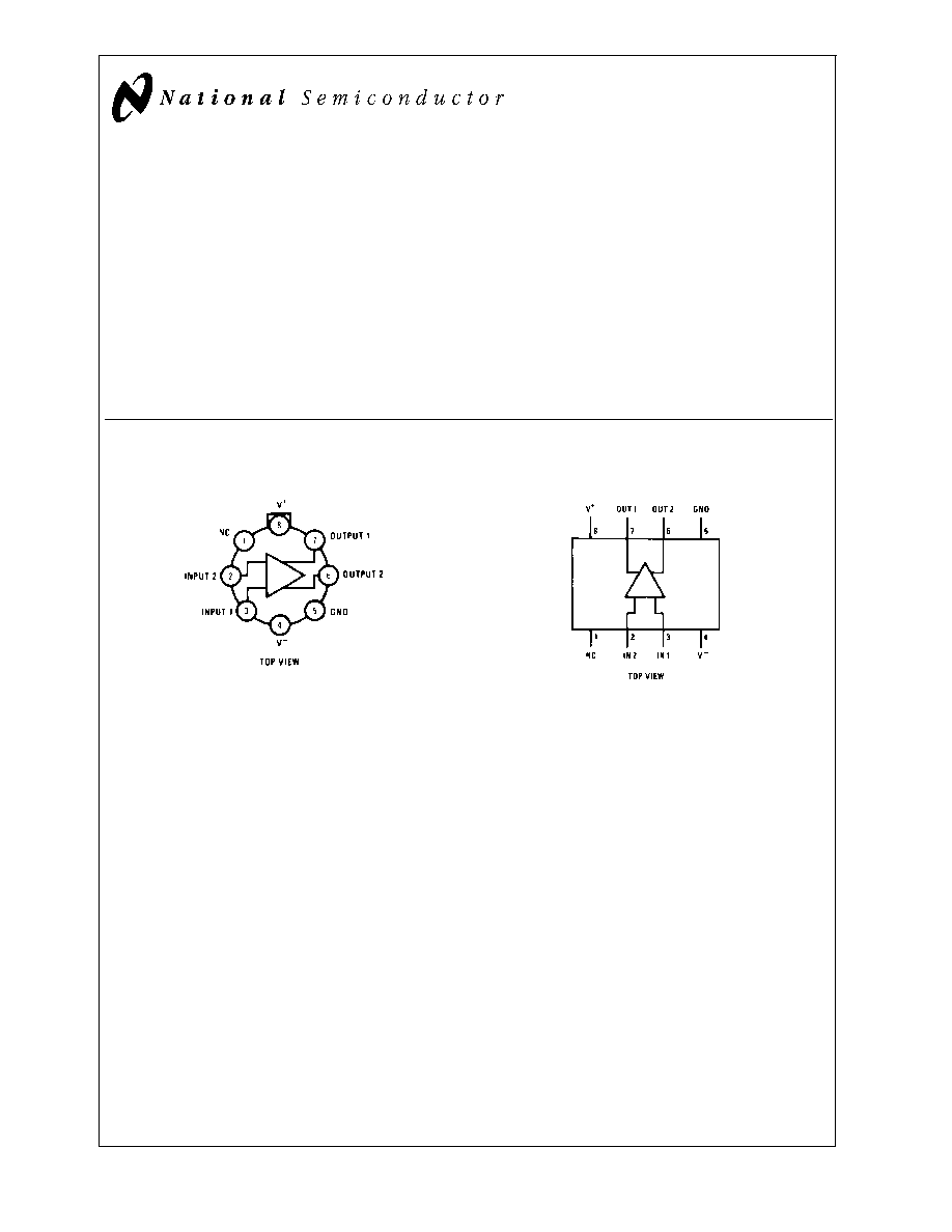
Connection Diagrams
Metal Can Package
DS005707-4
Order Number LM160H/883 (Note 1)
See NS Package Number H08C
Dual-In-Line Package
DS005707-5
Order Number LM360M, LM360MX or LM360N
See NS Package Number M08A or N08E
Note 1: Also available in SMD# 5962-8767401
August 2000
LM160/LM360
High
Speed
Differential
Comparator
© 2000 National Semiconductor Corporation
DS005707
www.national.com

Absolute Maximum Ratings
(Notes 6, 8)
If Military/Aerospace specified devices are required,
please contact the National Semiconductor Sales Office/
Distributors for availability and specifications.
Positive Supply Voltage
+8V
Negative Supply Voltage
-8V
Peak Output Current
20 mA
Differential Input Voltage
±
5V
Input Voltage
V
+
V
IN
V
-
ESD Tolerance (Note 9)
1600V
Operating Temperature Range
LM160
-55∞C to +125∞C
LM360
0∞C to +70∞C
Storage Temperature Range
-65∞C to +150∞C
Lead Temperature
(Soldering, 10 sec.)
260∞C
Soldering Information
Dual-In-Line Package
Soldering (10 seconds)
260∞C
Small Outline Package
Vapor Phase (60 seconds)
215∞C
Infrared (15 seconds)
220∞C
See AN-450 "Surface Mounting Methods and Their Effect
on Product Reliability" for other methods of soldering
surface mount devices.
Electrical Characteristics
(T
MIN
T
A
T
MAX
)
Parameter
Conditions
Min
Typ
Max
Units
Operating Conditions
Supply Voltage V
CC
+
4.5
5
6.5
V
Supply Voltage V
CC
-
-4.5
-5
-6.5
V
Input Offset Voltage
R
S
200
2
5
mV
Input Offset Current
0.5
3
µA
Input Bias Current
5
20
µA
Output Resistance (Either Output)
V
OUT
= V
OH
100
Response Time
T
A
= 25∞C, V
S
=
±
5V (Notes 2, 7)
13
25
ns
T
A
= 25∞C, V
S
=
±
5V (Notes 3, 7)
12
20
ns
T
A
= 25∞C, V
S
=
±
5V (Notes 4, 7)
14
ns
Response Time Difference between Outputs
(t
pd
of +V
IN1
) - (t
pd
of -V
IN2
)
T
A
= 25∞C (Notes 2, 7)
2
ns
(t
pd
of +V
IN2
) - (t
pd
of -V
IN1
)
T
A
= 25∞C (Notes 2, 7)
2
ns
(t
pd
of +V
IN1
) - (t
pd
of +V
IN2
)
T
A
= 25∞C (Notes 2, 7)
2
ns
(t
pd
of -V
IN1
) - (t
pd
of -V
IN2
)
T
A
= 25∞C (Notes 2, 7)
2
ns
Input Resistance
f = 1 MHz
17
k
Input Capacitance
f = 1 MHz
3
pF
Average Temperature Coefficient of
R
S
= 50
8
µV/∞C
Input Offset Voltage
Average Temperature Coefficient of
7
nA/∞C
Input Offset Current
Common Mode Input Voltage Range
V
S
=
±
6.5V
±
4
±
4.5
V
Differential Input Voltage Range
±
5
V
Output High Voltage (Either Output)
I
OUT
= -320 µA, V
S
=
±
4.5V
2.4
3
V
Output Low Voltage (Either Output)
I
SINK
= 6.4 mA
0.25
0.4
V
Positive Supply Current
V
S
=
±
6.5V
18
32
mA
Negative Supply Current
V
S
=
±
6.5V
-9
-16
mA
Note 2: Response time measured from the 50% point of a 30 mVp-p 10 MHz sinusoidal input to the 50% point of the output.
Note 3: Response time measured from the 50% point of a 2 Vp-p 10 MHz sinusoidal input to the 50% point of the output.
LM160/LM360
www.national.com
2
Electrical Characteristics
(Continued)
Note 4: Response time measured from the start of a 100 mV input step with 5 mV overdrive to the time when the output crosses the logic threshold.
Note 5: Typical thermal impedances are as follows:
Cavity DIP (J):
jA
135∞C/W
Header (H)
jA
165∞C/W
(Still Air)
Molded DIP (N):
jA
130∞C/W
67∞C/W
(400 LF/min Air Flow)
jC
25∞C/W
Note 6: The device may be damaged if used beyond the maximum ratings.
Note 7: Measurements are made in AC Test Circuit, Fanout = 1
Note 8: Refer to RETS 160X for LM160H, LM160J-14 and LM160J military specifications.
Note 9: Human body model, 1.5 k
in series with 100 pF.
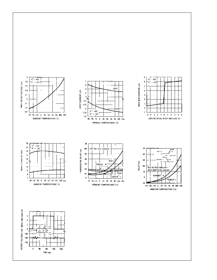
Typical Performance Characteristics
Offset Voltage
DS005707-8
Input Current vs Ambient
Temperature
DS005707-9
Input Characteristics
DS005707-10
Supply Current vs Ambient
Temperature
DS005707-11
Propagation Delay vs
Ambient Temperature
DS005707-12
Delay of Output 1 With
Respect to Output 2 vs
Ambient Temperature
DS005707-13
Common-Mode
Pulse Response
DS005707-14
LM160/LM360
www.national.com
3

AC Test Circuit
DS005707-3
V
IN
=
±
50 mV
FANOUT=1 FANOUT=4
V
+
=+5V
R=2.4k
R=630
V
-
=-5V
C=15 pF
C=30 pF
LM160/LM360
www.national.com
4
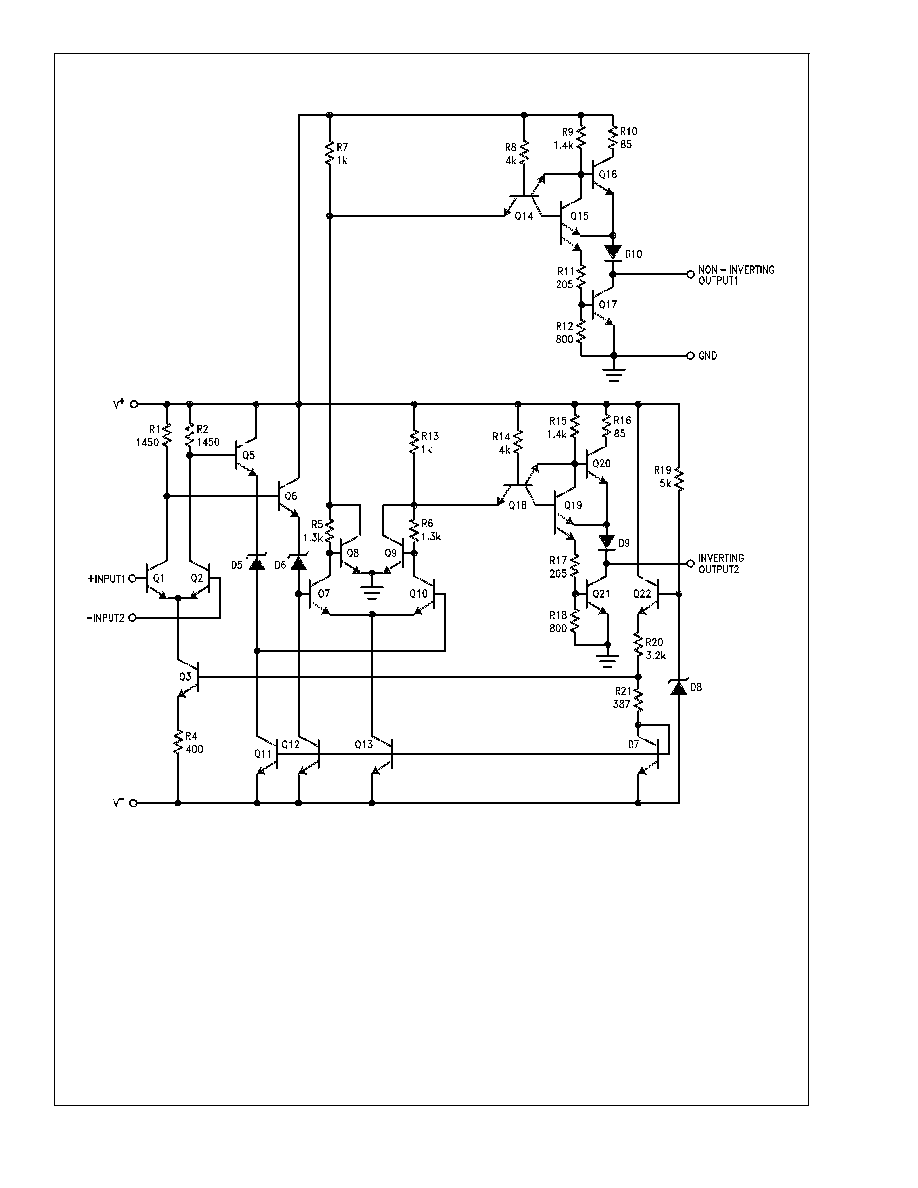
Schematic Diagram
DS005707-1
LM160/LM360
www.national.com
5