
TL H 7893
LM1815
Adaptive
Variable
Reluctance
Sensor
Amplifier
February 1995
LM1815 Adaptive Variable Reluctance Sensor Amplifier
General Description
The LM1815 is an adaptive sense amplifier and default gat-
ing circuit for motor control applications The sense amplifi-
er provides a one-shot pulse output whose leading edge
coincides with the negative-going zero crossing of a ground
referenced input signal such as from a variable reluctance
magnetic pick-up coil
In normal operation this timing reference signal is process-
ed (delayed) externally and returned to the LM1815 A logic
input is then able to select either the timing reference or the
processed signal for transmission to the output driver stage
The adaptive sense amplifier operates with a positive-going
threshold which is derived by peak detecting the incoming
signal and dividing this down Thus the input hysteresis var-
ies with input signal amplitude This enables the circuit to
sense in situations where the high speed noise is greater
than the low speed signal amplitude Minimum input signal
is 100 mVp-p
Features
Y
Adaptive hysteresis
Y
Single supply operation
Y
Ground referenced input
Y
True zero crossing timing reference
Y
Operates from 2V to 12V supply voltage
Y
Handles inputs from 100 mV to over 120V with external
resistor
Y
CMOS compatible logic
Applications
Y
Position sensing with notched wheels
Y
Zero crossing switch
Y
Motor speed control
Y
Tachometer
Y
Engine testing
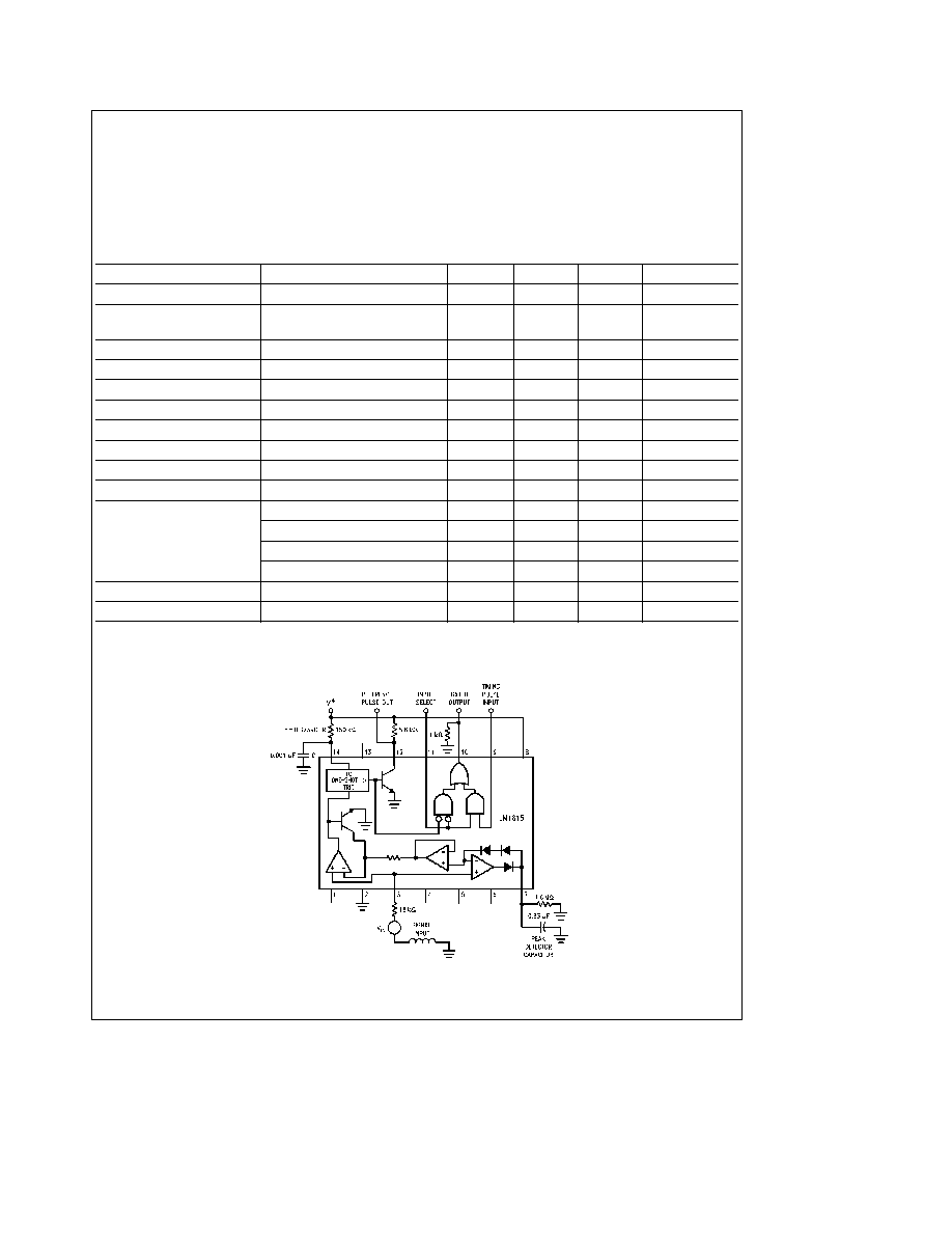
Connection Diagram
TL H 7893 � 1
Top View
Order Number LM1815M or LM1815N
See NS Package Number M14A or N14A
Truth Table
Signal
Input
Timing
Gated
Input
Select
Input
Output
Pulses
L
X
Pulses
X
H
Pulses
Pulses
C1995 National Semiconductor Corporation
RRD-B30M115 Printed in U S A
Absolute Maximum Ratings
If Military Aerospace specified devices are required
please contact the National Semiconductor Sales
Office Distributors for availability and specifications
Supply Voltage
12V
Power Dissipation (Note 1)
1250 mW
Operating Temperature Range
b
40 C to
a
125 C
Storage Temperature Range
b
65 C to
a
150 C
Junction Temperature (Note 2)
a
125 C
Input Current
g
30 mA
Lead Temperature (Soldering 10 sec )
260 C
Electrical Characteristics
(T
A
e
25 C V
CC
e
10V unless otherwise specified see
Figure 1 )
Parameter
Conditions
Min
Typ
Max
Units
Operating Supply Voltage
2 5
10
12
V
Supply Current
f
IN
e
500 Hz Pin 9
e
2V
3 6
6
mA
Pin 11
e
0 8V
Reference Pulse Width
f
IN
e
1 Hz to 2 kHz
70
100
130
m
s
Input Bias Current
V
IN
e
2V (Pin 9 and Pin 11)
5
m
A
Input Bias Current
V
IN
e
0V dc (Pin 3)
200
nA
Input Impedance
V
IN
e
5 Vrms (Note 3)
12
20
28
kX
Zero Crossing Threshold
V
IN
e
100 mVp-p (Pin 3)
25
mV
Logic Threshold
(Pin 9 and Pin 11)
0 8
1 1
2 0
V
V
OUT
High
R
L
e
1 kX (Pin 10)
7 5
8 6
V
V
OUT
Low
I
SINK
e
0 1 mA (Pin 10)
0 3
0 4
V
Input Arming Threshold
Pin 5 Open V
IN
s
135 mVp-p
30
45
60
mV
Pin 5 Open V
IN
t
230 mVp-p
40
80
90
% of V
3
Pk
Pin 5 to V
a
200
mV
Pin 5 to Gnd
b
25
25
mV
Output Leakage Pin 12
V
12
e
11V
0 01
10
m
A
Saturation Voltage P12
I
12
e
2 mA
0 2
0 4
V
Note 1
For operation at elevated temperatures the device must be derated based on a 125 C maximum junction temperature and a thermal resistance of 80 C W
(DIP) 120 C W (SO-14) junction to ambient
Note 2
Temporary excursions to 150 C can be tolerated
Note 3
Measured at input to external 18 kX resistor IC contains 1 kX in series with a diode to attenuate the input signal
TL H 7893 � 2
FIGURE 1 LM1815 Adaptive Sense Amplifier
2
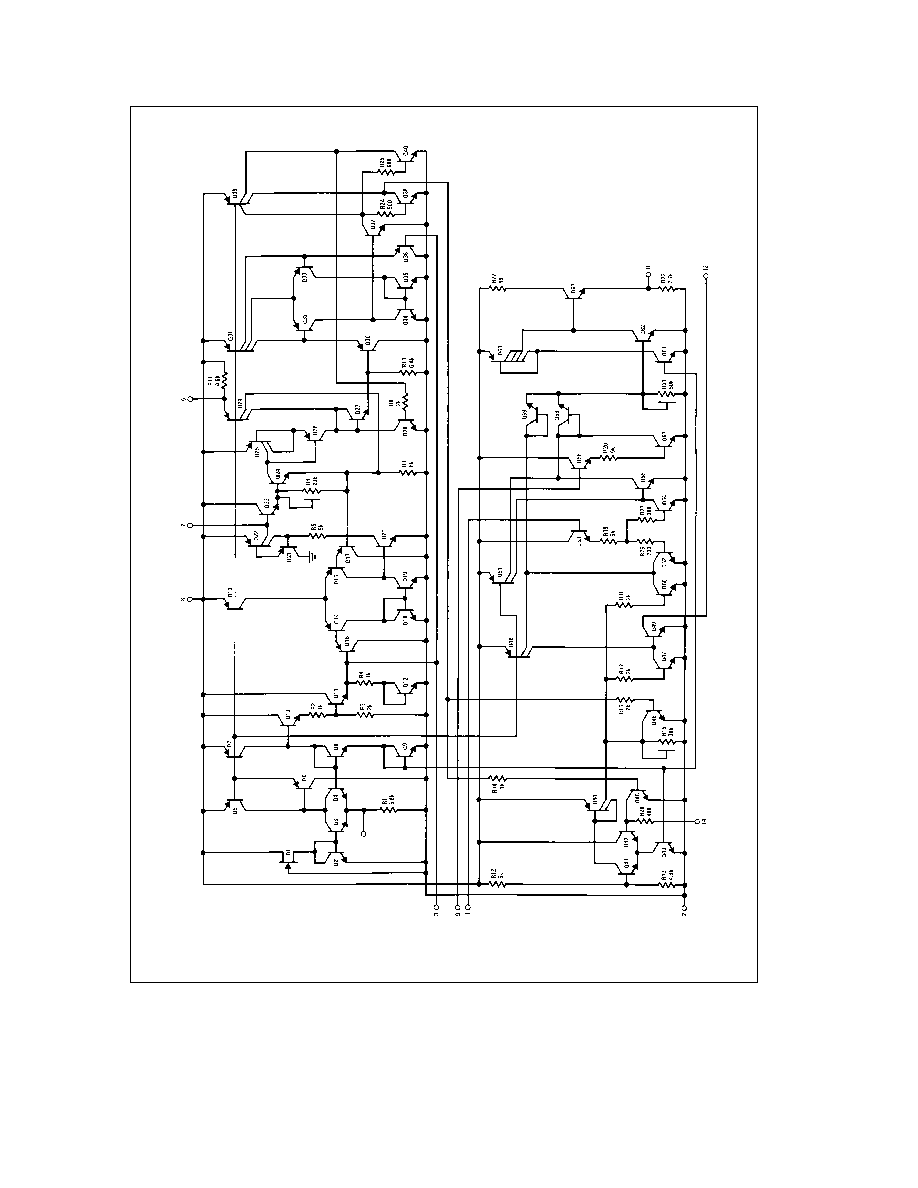
Schematic Diagram
TL H 7893 � 4
3

TL H 7893 � 3
FIGURE 2 LM1815 Oscillograms
Application Hints
Input Clamp
The signal input at pin 3 is internally clamped Current limit
is provided by an external resistor which should be selected
to allow a peak current of 3 mA in normal operation Positive
inputs are clamped by a 1 kX resistor and series diode
while an active clamp limits pin 3 to
b
350 mV for negative
inputs (see R4 Q12 Q11 in internal schematic diagram)
Operation of Zero Crossing Detector
The LM1815 is designed to operate as a zero crossing de-
tector triggering an internal one shot on the negative-going
edge of the input signal Unlike other zero crossing detec-
tors the LM1815 cannot be triggered until the input signal
has crossed an ``arming'' threshold on the positive-going
portion of the waveform The arming circuit is reset when
the chip is triggered and subsequent zero crossings are
ignored until the arming threshold is exceeded again This
threshold varies depending on the connection at pin 5
Three different modes of operation are possible
MODE 1 Pin 5 open
The adaptive mode is selected by
leaving pin 5 open circuit For input signals of less than
135 mVp-p the input arming threshold is typically 45 mV
Under these conditions the input signal must first cross the
45 mV threshold in the positive direction to arm the zero
crossing detector and then cross zero in the negative direc-
tion to trigger it If the signal is less than 30 mV peak (mini-
mum rating in Electrical Characteristics) the one shot is
guaranteed to not trigger
Input signals of greater than 230 mVp-p cause the arming
threshold to track at 80% of the peak input voltage A peak
detector (pin 7) stores a value relative to the positive input
peaks to establish the arming threshold Input signals must
exceed this threshold in the positive direction to arm the
zero crossing detector which can then be triggered by a
negative-going zero crossing The peak detector tracks rap-
idly as the input signal amplitude increases and decays by
virtue of the resistor connected externally at pin 7 to track
decreases in the input signal
Note that since the input is clamped the waveform ob-
served at pin 3 is not identical to the waveform observed at
the variable reluctance sensor Similarly the voltage stored
at pin 7 is not identical to the peak voltage appearing at
pin 3
MODE 2 Pin 5 connected to V
a
The input arming thresh-
old is fixed at 200 mV minimum when pin 5 is connected to
the positive supply The chip has no output for signals of
less than 200 mV peak and triggers on the next negative-
going zero crossing when the threshold is exceeded
MODE 3 Pin 5 grounded
With pin 5 grounded the input
arming threshold is set to 0V (
g
25 mV maximum) Positive-
going zero crossings arm the chip and the next negative
zero crossing triggers it
The one shot timing is set by a resistor and capacitor con-
nected to pin 14 The output pulse width is
pulse width
e
0 673 RC
(1)
In some systems it is necessary to externally generate puls-
es such as during stall conditions when the variable reluc-
tance sensor has no output External pulse inputs at pin 9
are gated through to pin 10 when Input Select (pin 11) is
pulled high Pin 12 is a direct output for the one shot and is
unaffected by the status of pin 11
Input output pins 9 11 10 and 12 are all CMOS logic com-
patible In addition pins 9 11 and 12 are TTL compatible
Pin 10 is not guaranteed to drive a TTL load
Pins 1 4 6 and 13 have no internal connections and can be
grounded
4

Physical Dimensions
inches (millimeters)
14-Lead Small Outline Integrated Circuit (M)
Order Number LM1815M
NS Package Number M14A
5

LM1815
Adaptive
Variable
Reluctance
Sensor
Amplifier
Physical Dimensions
inches (millimeters) (Continued)
Molded Dual-In-Line Package (N)
Order Number LM1815N
NS Package Number N14A
LIFE SUPPORT POLICY
NATIONAL'S PRODUCTS ARE NOT AUTHORIZED FOR USE AS CRITICAL COMPONENTS IN LIFE SUPPORT
DEVICES OR SYSTEMS WITHOUT THE EXPRESS WRITTEN APPROVAL OF THE PRESIDENT OF NATIONAL
SEMICONDUCTOR CORPORATION As used herein
1 Life support devices or systems are devices or
2 A critical component is any component of a life
systems which (a) are intended for surgical implant
support device or system whose failure to perform can
into the body or (b) support or sustain life and whose
be reasonably expected to cause the failure of the life
failure to perform when properly used in accordance
support device or system or to affect its safety or
with instructions for use provided in the labeling can
effectiveness
be reasonably expected to result in a significant injury
to the user
National Semiconductor
National Semiconductor
National Semiconductor
National Semiconductor
Corporation
Europe
Hong Kong Ltd
Japan Ltd
1111 West Bardin Road
Fax (a49) 0-180-530 85 86
13th Floor Straight Block
Tel 81-043-299-2309
Arlington TX 76017
Email cnjwge tevm2 nsc com
Ocean Centre 5 Canton Rd
Fax 81-043-299-2408
Tel 1(800) 272-9959
Deutsch Tel (a49) 0-180-530 85 85
Tsimshatsui Kowloon
Fax 1(800) 737-7018
English
Tel (a49) 0-180-532 78 32
Hong Kong
Fran ais Tel (a49) 0-180-532 93 58
Tel (852) 2737-1600
Italiano
Tel (a49) 0-180-534 16 80
Fax (852) 2736-9960
National does not assume any responsibility for use of any circuitry described no circuit patent licenses are implied and National reserves the right at any time without notice to change said circuitry and specifications