LM1875
20W Audio Power Amplifier
General Description
The LM1875 is a monolithic power amplifier offering very low
distortion and high quality performance for consumer audio
applications.
The LM1875 delivers 20 watts into a 4
or 8
load on
±
25V
supplies. Using an 8
load and
±
30V supplies, over 30
watts of power may be delivered. The amplifier is designed
to operate with a minimum of external components. Device
overload protection consists of both internal current limit and
thermal shutdown.
The LM1875 design takes advantage of advanced circuit
techniques and processing to achieve extremely low distor-
tion levels even at high output power levels. Other outstand-
ing features include high gain, fast slew rate and a wide
power bandwidth, large output voltage swing, high current
capability, and a very wide supply range. The amplifier is in-
ternally compensated and stable for gains of 10 or greater.
Features
n
Up to 30 watts output power
n
A
VO
typically 90 dB
n
Low distortion: 0.015%, 1 kHz, 20 W
n
Wide power bandwidth: 70 kHz
n
Protection for AC and DC short circuits to ground
n
Thermal protection with parole circuit
n
High current capability: 4A
n
Wide supply range 16V-60V
n
Internal output protection diodes
n
94 dB ripple rejection
n
Plastic power package TO-220
Applications
n
High performance audio systems
n
Bridge amplifiers
n
Stereo phonographs
n
Servo amplifiers
n
Instrument systems
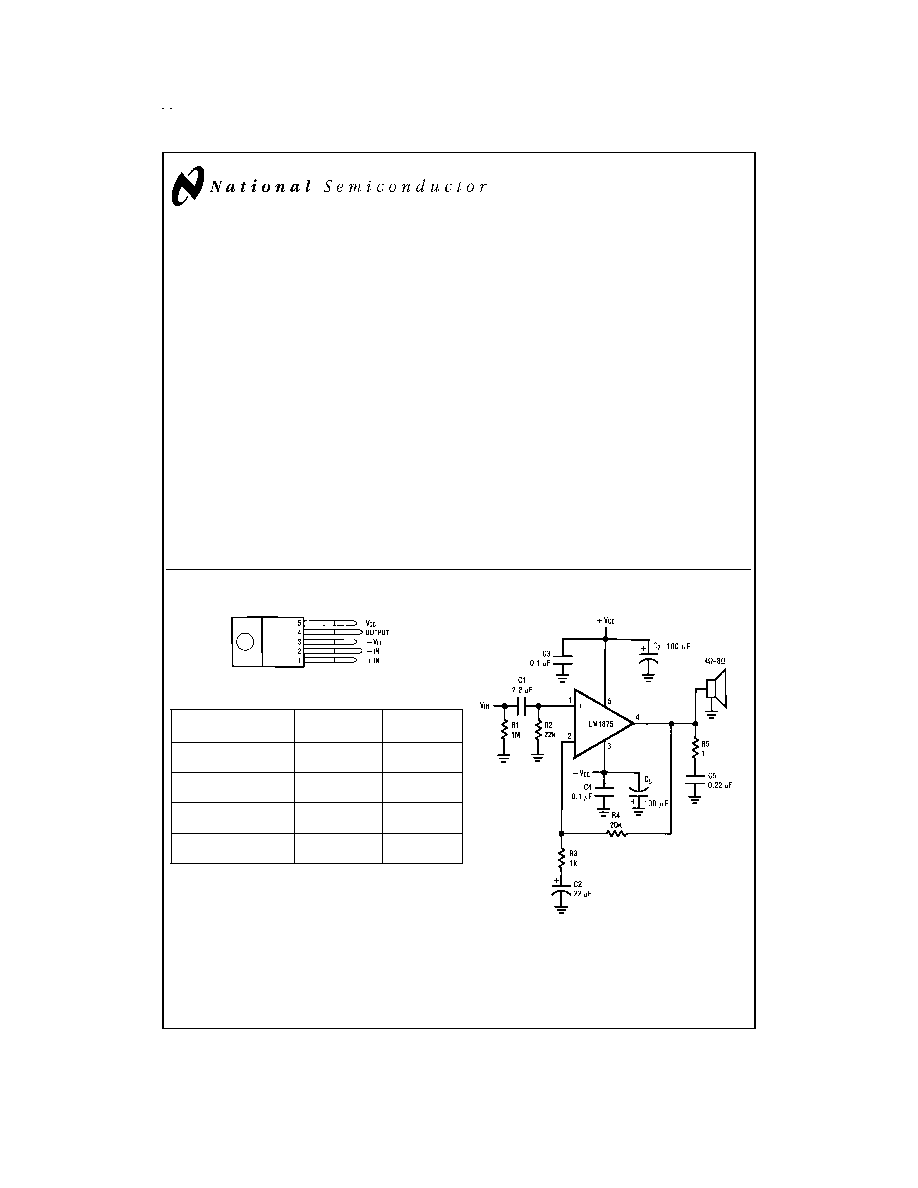
Connection Diagram
Package
Ordering Info
NSC Package
Number
For Straight Leads
LM1875T
SL108949
T05A
For Stagger Bend
LM1875T
LB03
T05D
For 90∞ Stagger Bend
LM1875T
LB05
T05E
For 90∞ Stagger Bend
LM1875T
LB02
TA05B
Typical Applications
DS005030-1
Front View
DS005030-2
February 1999
LM1875
20W
Audio
Power
Amplifier
© 1999 National Semiconductor Corporation
DS005030
www.national.com

Absolute Maximum Ratings
(Note 1)
Supply Voltage
60V
Input Voltage
-V
EE
to V
CC
Storage Temperature
-65∞C to + 150∞C
Junction Temperature
150∞C
Lead Temperature
(Soldering, 10 seconds)
260∞C
JC
3∞C
JA
73∞C
Electrical Characteristics
V
CC
=+25V, -V
EE
=-25V, T
AMBIENT
=25∞C, R
L
=8
, A
V
=20 (26 dB), f
o
=1 kHz, unless otherwise specified.
Parameter
Conditions
Typical
Tested Limits
Units
Supply Current
P
OUT
=0W
70
100
mA
Output Power (Note 2)
THD=1%
25
W
THD (Note 2)
P
OUT
=20W, f
o
=1 kHz
0.015
%
P
OUT
=20W, f
o
=20 kHz
0.05
0.4
%
P
OUT
=20W, R
L
=4
, f
o
=1 kHz
0.022
%
P
OUT
=20W, R
L
=4
, f
o
=20 kHz
0.07
0.6
%
Offset Voltage
±
1
±
15
mV
Input Bias Current
±
0.2
±
2
µA
Input Offset Current
0
±
0.5
µA
Gain-Bandwidth Product
f
o
=20 kHz
5.5
MHz
Open Loop Gain
DC
90
dB
PSRR
V
CC
, 1 kHz, 1 Vrms
95
52
dB
V
EE
, 1 kHz, 1 Vrms
83
52
dB
Max Slew Rate
20W, 8
, 70 kHz BW
8
V/µs
Current Limit
V
OUT
= V
SUPPLY
-10V
4
3
A
Equivalent Input Noise Voltage
R
S
=600
, CCIR
3
µVrms
Note 1: "Absolute Maximum Ratings" indicate limits beyond which damage to the device may occur. Operating Ratings indicate conditions for which the device is
functional, but do not guarantee specific performance limits.
Note 2: Assumes the use of a heat sink having a thermal resistance of 1∞C/W and no insulator with an ambient temperature of 25∞C. Because the output limiting
circuitry has a negative temperature coefficient, the maximum output power delivered to a 4
load may be slightly reduced when the tab temperature exceeds 55∞C.
Typical Applications
Typical Single Supply Operation
DS005030-3
www.national.com
2
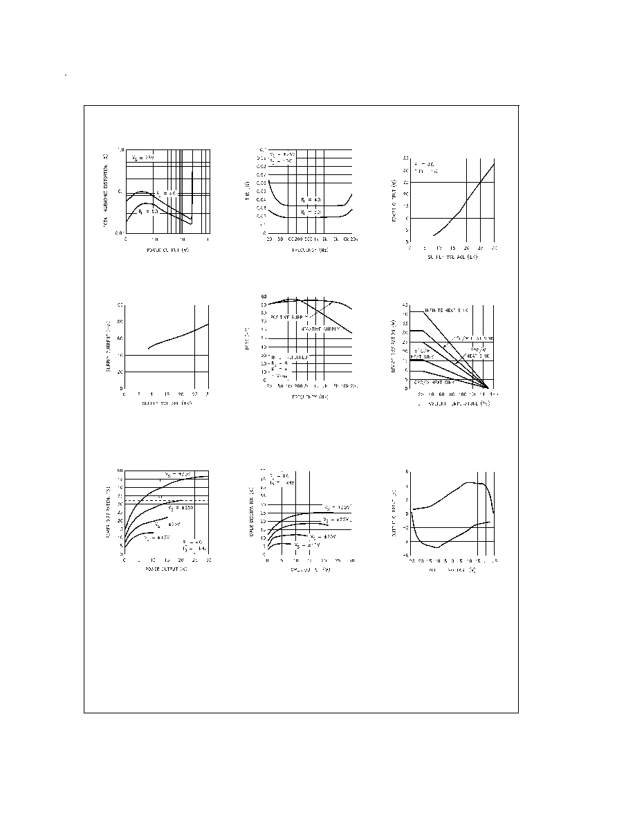
Typical Performance Characteristics
THD vs Power Output
DS005030-9
THD vs Frequency
DS005030-10
Power Output vs Supply
Voltage
DS005030-11
Supply Current vs Supply
Voltage
DS005030-12
PSRR vs Frequency
DS005030-13
Device Dissipation vs
Ambient Temperature
DS005030-14
INTERFACE = 1∞C/W.
See Application Hints.
Power Dissipation vs
Power Output
DS005030-15
Power Dissipation vs
Power Output
DS005030-16
I
OUT
vs V
OUT
-Current Limit/
Safe Operating Area Boundary
DS005030-17
www.national.com
3

Typical Performance Characteristics
(Continued)
Open Loop Gain and
Phase vs Frequency
DS005030-18
Note 3: Thermal shutdown with infinite heat sink
Note 4: Thermal shutdown with 1∞C/W heat sink
Input Bias Current
vs Supply Voltage
DS005030-19
www.national.com
4
