LM1881, LM1881-X
Video Sync Separator
General Description
The LM1881 Video sync separator extracts timing informa-
tion including composite and vertical sync, burst/back porch
timing, and odd/even field information from standard nega-
tive going sync NTSC, PAL* and SECAM video signals with
amplitude from 0.5V to 2V p-p. The integrated circuit is also
capable of providing sync separation for non-standard,
faster horizontal rate video signals. The vertical output is
produced on the rising edge of the first serration in the
vertical sync period. A default vertical output is produced
after a time delay if the rising edge mentioned above does
not occur within the externally set delay period, such as
might be the case for a non-standard video signal.
Features
n
AC coupled composite input signal
n
>
10 k
input resistance
n
<
10 mA power supply drain current
n
Composite sync and vertical outputs
n
Odd/even field output
n
Burst gate/back porch output
n
Horizontal scan rates to 150 kHz
n
Edge triggered vertical output
n
Default triggered vertical output for non-standard video
signal (video games-home computers)
n
-40∞C to +85∞C operation (LM1881-X)
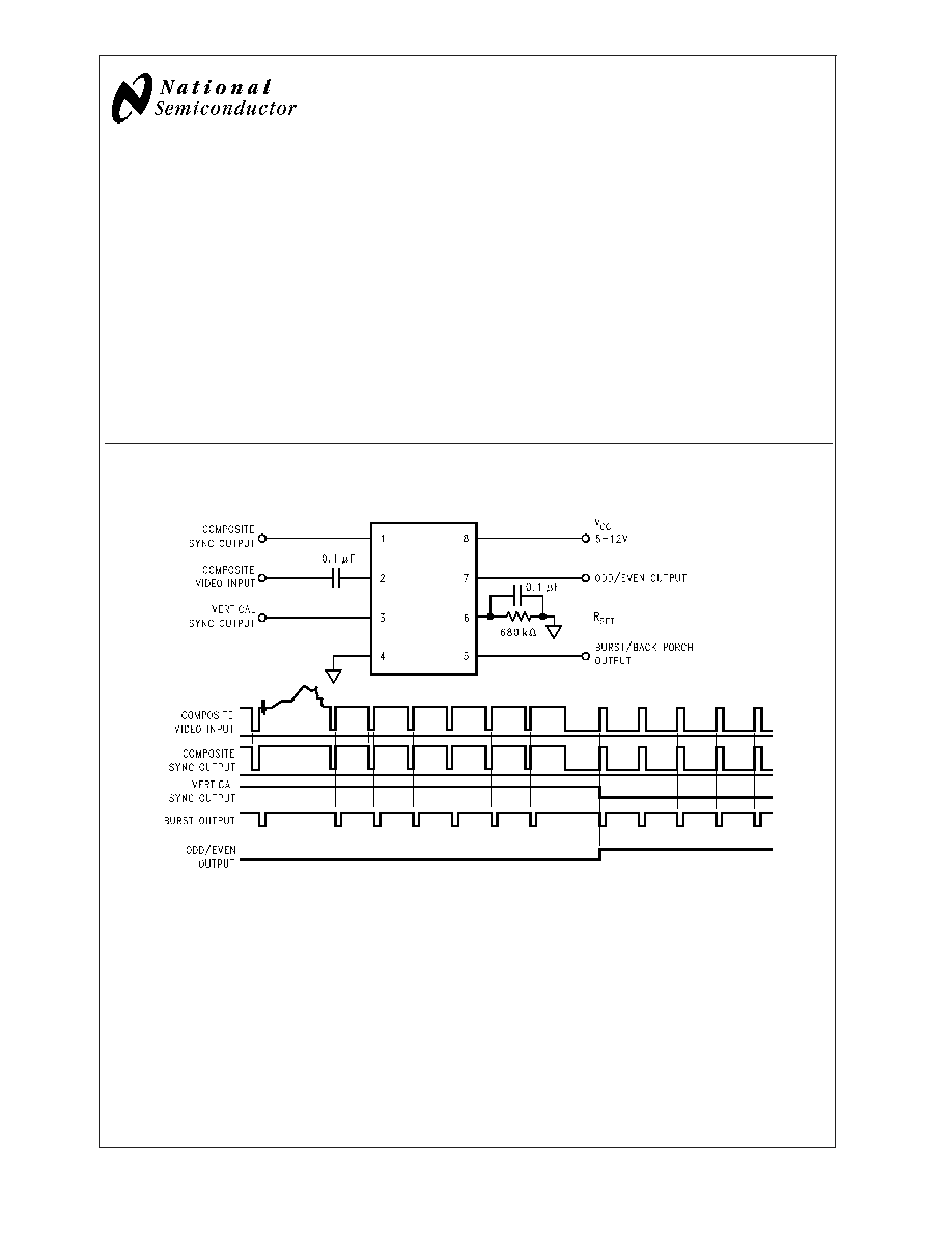
Connection Diagram
LM1881N
00915001
Order Number LM1881M or LM1881N (0∞C to +70∞C)
Order Number LM1881M-X or LM1881N-X (-40∞C to +85∞C)
See NS Package Number M08A or N08E
*PAL in this datasheet refers to European broadcast TV standard "Phase Alternating Line", and not to Programmable Array Logic.
June 2003
LM1881,
LM1881-X
V
ideo
Sync
Separator
© 2003 National Semiconductor Corporation
DS009150
www.national.com
Absolute Maximum Ratings
(Note 1)
If Military/Aerospace specified devices are required,
please contact the National Semiconductor Sales Office/
Distributors for availability and specifications.
Supply Voltage
13.2V
Input Voltage
3 V
P-P
(V
CC
= 5V)
6 V
P-P
(V
CC
8V)
Output Sink Currents; Pins, 1, 3, 5
5 mA
Output Sink Current; Pin 7
2 mA
Package Dissipation (Note 2)
1100 mW
Storage Temperature Range
-65∞C to +150∞C
ESD Susceptibility (Note 3)
2 kV
Soldering Information
Dual-In-Line Package (10 sec.)
260∞C
Small Outline Package
Vapor Phase (60 sec.)
215∞C
Infrared (15 sec.)
220∞C
Electrical Characteristics LM1881
V
CC
= 5V; R
SET
= 680 k
; T
A
= 0∞C to +70∞C by correlation with 100% electrical testing at T
A
=25∞C
Parameter
Conditions
Min
Typ (Note 4)
Max
Units
Supply Current
Outputs at
Logic 1
V
CC
= 5V
V
CC
= 12V
5.2
5.5
10
12
mA
DC Input Voltage
Pin 2
1.3
1.5
1.8
V
Input Threshold Voltage
(Note 5)
55
70
85
mV
Input Discharge Current
Pin 2; V
IN
= 2V
6
11
16
µA
Input Clamp Charge Current
Pin 2; V
IN
= 1V
0.2
0.8
mA
R
SET
Pin Reference Voltage
Pin 6; (Note 6)
1.10
1.22
1.35
V
Composite Sync. & Vertical
Outputs
I
OUT
= 40 µA;
Logic 1
V
CC
= 5V
V
CC
= 12V
4.0
11.0
4.5
V
I
OUT
= 1.6 mA
Logic 1
V
CC
= 5V
V
CC
= 12V
2.4
10.0
3.6
V
Burst Gate & Odd/Even
Outputs
I
OUT
= 40 µA;
Logic 1
V
CC
= 5V
V
CC
= 12V
4.0
11.0
4.5
V
Composite Sync. Output
I
OUT
= -1.6 mA; Logic 0; Pin 1
0.2
0.8
V
Vertical Sync. Output
I
OUT
= -1.6 mA; Logic 0; Pin 3
0.2
0.8
V
Burst Gate Output
I
OUT
= -1.6 mA; Logic 0; Pin 5
0.2
0.8
V
Odd/Even Output
I
OUT
= -1.6 mA; Logic 0; Pin 7
0.2
0.8
V
Vertical Sync Width
190
230
300
µs
Burst Gate Width
2.7 k
from Pin 5 to V
CC
2.5
4
4.7
µs
Vertical Default Time
(Note 7)
32
65
90
µs
LM1881,
LM1881-X
www.national.com
2
Electrical Characteristics LM1881≠X
V
CC
= 5V; R
SET
= 680 k
; T
A
= ≠40∞C to +85∞C by correlation with 100% electrical testing at T
A
=25∞C
Parameter
Conditions
Min
Typ
Max
Units
Supply Current
Outputs at
Logic 1
V
CC
= 5V
V
CC
= 12V
5.2
5.5
10
12
mA
DC Input Voltage
Pin 2
1.3
1.5
1.8
V
Input Threshold Voltage
55
70
85
mV
Input Discharge Current
Pin 2; V
IN
= 2V
6
11
16
µA
Input Clamp Charge Current
Pin 2; V
IN
= 1V
0.2
0.8
mA
R
SET
Pin Reference Voltage
Pin 6;
1.10
1.22
1.35
V
Composite Sync. & Vertical
Outputs
I
OUT
= 40 µA;
Logic 1
V
CC
= 5V
V
CC
= 12V
4.0
11.0
4.5
V
I
OUT
= 1.6 mA
Logic 1
V
CC
= 5V
V
CC
= 12V
2.4
10.0
3.6
V
Burst Gate & Odd/Even
Outputs
I
OUT
= 40 µA;
Logic 1
V
CC
= 5V
V
CC
= 12V
4.0
11.0
4.5
V
Composite Sync. Output
I
OUT
= -1.6 mA; Logic 0; Pin 1
0.2
0.8
V
Vertical Sync. Output
I
OUT
= -1.6 mA; Logic 0; Pin 3
0.2
0.8
V
Burst Gate Output
I
OUT
= -1.6 mA; Logic 0; Pin 5
0.2
0.8
V
Odd/Even Output
I
OUT
= -1.6 mA; Logic 0; Pin 7
0.2
0.8
V
Vertical Sync Width
140
230
588
µs
Burst Gate Width
2.7 k
from Pin 5 to V
CC
2.2
4
4.7
µs
Vertical Default Time
32
65
90
µs
Note 1: Absolute Maximum Ratings indicate limits beyond which damage to the device may occur. For guaranteed specifications and test conditions, see the
Electrical Characteristics. The guaranteed specifications apply only for the test conditions listed.
Note 2: For operation in ambient temperatures above 25∞C, the device must be derated based on a 150∞C maximum junction temperature and a package thermal
resistance of 110∞C/W, junction to ambient.
Note 3: ESD susceptibility test uses the "human body model, 100 pF discharged through a 1.5 k
resistor".
Note 4: Typicals are at T
J
= 25∞C and represent the most likely parametric norm.
Note 5: Relative difference between the input clamp voltage and the minimum input voltage which produces a horizontal output pulse.
Note 6: Careful attention should be made to prevent parasitic capacitance coupling from any output pin (Pins 1, 3, 5 and 7) to the R
SET
pin (Pin 6).
Note 7: Delay time between the start of vertical sync (at input) and the vertical output pulse.
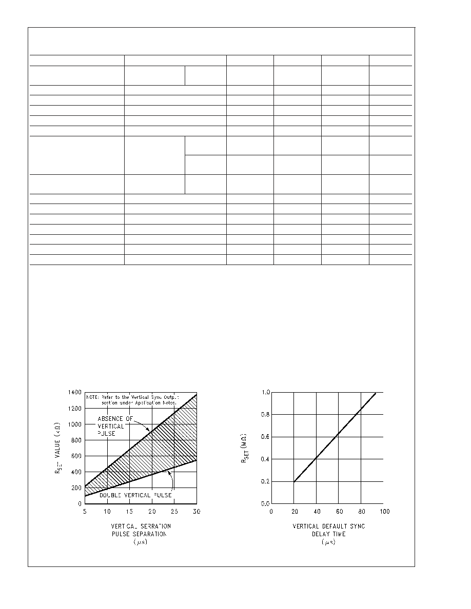
Typical Performance Characteristics
R
SET
Value Selection
vs Vertical Serration
Pulse Separation
Vertical Default
Sync Delay Time
vs R
SET
00915007
00915008
LM1881,
LM1881-X
www.national.com
3
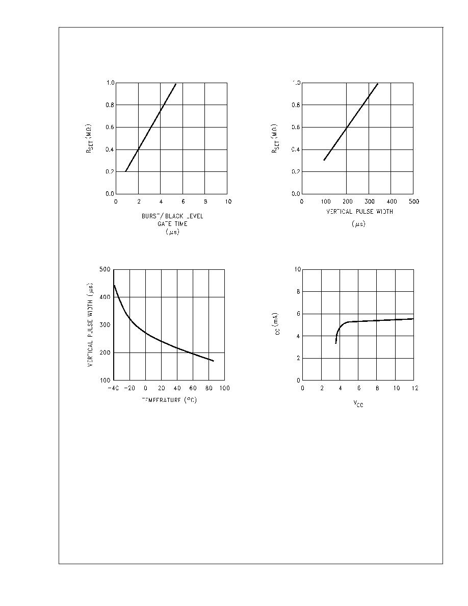
Typical Performance Characteristics
(Continued)
Burst/Black Level
Gate Time vs R
SET
Vertical Pulse
Width vs R
SET
00915009
00915010
Vertical Pulse
Width vs Temperature
Supply Current vs
Supply Voltage
00915011
00915002
Application Notes
The LM1881 is designed to strip the synchronization signals
from composite video sources that are in, or similar to, the
N.T.S.C. format. Input signals with positive polarity video
(increasing signal voltage signifies increasing scene bright-
ness) from 0.5V (p-p) to 2V (p-p) can be accommodated.
The LM1881 operates from a single supply voltage between
5V DC and 12V DC. The only required external components
besides a power supply decoupling capacitor at pin 8 and a
set current decoupling capacitor at pin 6, are the composite
input coupling capacitor at pin 2 and one resistor at pin 6 that
sets internal current levels. The resistor on pin 6 (i.e. R
set
)
allows the LM1881 to be adjusted for source signals with line
scan frequencies differing from 15.734 kHz. Four major sync
signals are available from the I/C; composite sync including
both horizontal and vertical scan timing information; a verti-
cal sync pulse; a burst gate or back porch clamp pulse; and
an odd/even output. The odd/even output level identifies
which video field of an interlaced video source is present at
the input. The outputs from the LM1881 can be used to
gen-lock video camera/VTR signals with graphics sources,
provide identification of video fields for memory storage,
recover suppressed or contaminated sync signals, and pro-
vide timing references for the extraction of coded or uncoded
data on specific video scan lines.
To better understand the LM1881 timing information and the
type of signals that are used, refer to Figure 1(a-e) which
shows a portion of the composite video signal from the end
of one field through the beginning of the next field.
LM1881,
LM1881-X
www.national.com
4

Application Notes
(Continued)
COMPOSITE SYNC OUTPUT
The composite sync output, Figure 1(b), is simply a repro-
duction of the signal waveform below the composite video
black level, with the video completely removed. This is ob-
tained by clamping the video signal sync tips to 1.5V DC at
Pin 2 and using a comparator threshold set just above this
voltage to strip the sync signal, which is then buffered out to
Pin 1. The threshold separation from the clamped sync tip is
nominally 70 mV which means that for the minimum input
level of 0.5V (p-p), the clipping level is close to the halfway
point on the sync pulse amplitude (shown by the dashed line
on Figure 1(a). This threshold separation is independent of
the signal amplitude, therefore, for a 2V (p-p) input the
clipping level occurs at 11% of the sync pulse amplitude. The
charging current for the input coupling capacitor is 0.8 mA,
Normally the signal source for the LM1881 is assumed to be
clean and relatively noise-free, but some sources may have
excessive video peaking, causing high frequency video and
chroma components to extend below the black level refer-
ence. Some video discs keep the chroma burst pulse
present throughout the vertical blanking period so that the
burst actually appears on the sync tips for three line periods
instead of at black level. A clean composite sync signal can
be generated from these sources by filtering the input signal.
When the source impedance is low, typically 75
, a 620
resistor in series with the source and a 510 pF capacitor to
ground will form a low pass filter with a corner frequency of
500 kHz. This bandwidth is more than sufficient to pass the
sync pulse portion of the waveform; however, any subcarrier
content in the signal will be attenuated by almost 18 dB,
effectively taking it below the comparator threshold. Filtering
will also help if the source is contaminated with thermal
noise. The output waveforms will become delayed from be-
tween 40 ns to as much as 200 ns due to this filter. This
much delay will not usually be significant but it does contrib-
ute to the sync delay produced by any additional signal
processing. Since the original video may also undergo pro-
cessing, the need for time delay correction will depend on
the total system, not just the sync stripper.
VERTICAL SYNC OUTPUT
A vertical sync output is derived by internally integrating the
composite sync waveform (Figure 2). To understand the
generation of the vertical sync pulse, refer to the lower left
hand section Figure 2. Note that there are two comparators
in the section. One comparator has an internally generated
voltage reference called V
1
going to one of its inputs. The
other comparator has an internally generated voltage refer-
ence called V
2
going to one of its inputs. Both comparators
have a common input at their noninverting input coming from
the internal integrator. The internal integrator is used for
integrating the composite sync signal. This signal comes
from the input side of the composite sync buffer and are
positive going sync pulses. The capacitor to the integrator is
internal to the LM1881. The capacitor charge current is set
by the value of the external resistor R
SET
. The output of the
integrator is going to be at a low voltage during the normal
horizontal lines because the integrator has a very short time
to charge the capacitor, which is during the horizontal sync
period. The equalization pulses will keep the output voltage
of the integrator at about the same level, below the V
1
.
During the vertical sync period the narrow going positive
pulses shown in Figure 1 is called the serration pulse. The
wide negative portion of the vertical sync period is called the
vertical sync pulse. At the start of the vertical sync period,
before the first Serration pulse occurs, the integrator now
charges the capacitor to a much higher voltage. At the first
serration pulse the integrator output should be between V
1
and V
2
. This would give a high level at the output of the
comparator with V
1
as one of its inputs. This high is clocked
into the "D" flip-flop by the falling edge of the serration pulse
(remember the sync signal is inverted in this section of the
LM1881). The "Q" output of the "D" flip-flop goes through the
OR gate, and sets the R/S flip-flop. The output of the R/S
flip-flop enables the internal oscillator and also clocks the
ODD/EVEN "D" flip-flop. The ODD/EVEN field pulse opera-
tion is covered in the next section. The output of the oscilla-
tor goes to a divide by 8 circuit, thus resetting the R/S
flip-flop after 8 cycles of the oscillator. The frequency of the
oscillator is established by the internal capacitor going to the
oscillator and the external R
SET
. The "Q" output of the R/S
flip-flop goes to pin 3 and is the actual vertical sync output of
the LM1881. By clocking the "D" flip-flop at the start of the
first serration pulse means that the vertical sync output pulse
starts at this point in time and lasts for eight cycles of the
internal oscillator as shown in Figure 1.
How R
SET
affects the integrator and the internal oscillator is
shown under the Typical Performance Characteristics. The
first graph is "R
SET
Value Selection vs Vertical Serration
Pulse Separation". For this graph to be valid, the vertical
sync pulse should last for at least 85% of the horizontal half
line (47% of a full horizontal line). A vertical sync pulse from
any standard should meet this requirement; both NTSC and
PAL do meet this requirement (the serration pulse is the
remainder of the period, 10% to 15% of the horizontal half
line). Remember this pulse is a positive pulse at the integra-
tor but negative in Figure 1. This graph shows how long it
takes the integrator to charge its internal capacitor above V
1
.
With R
SET
too large the charging current of the integrator will
be too small to charge the capacitor above V
1
, thus there will
be no vertical synch output pulse. As mentioned above, R
SET
also sets the frequency of the internal oscillator. If the oscil-
lator runs too fast its eight cycles will be shorter than the
vertical sync portion of the composite sync. Under this con-
dition another vertical sync pulse can be generated on one of
the later serration pulse after the divide by 8 circuit resets the
R/S flip-flop. The first graph also shows the minimum R
SET
necessary to prevent a double vertical pulse, assuming that
the serration pulses last for only three full horizontal line
periods (six serration pulses for NTSC). The actual pulse
width of the vertical sync pulse is shown in the "Vertical
Pulse Width vs R
SET
" graph. Using NTSC as an example,
lets see how these two graphs relate to each other. The
Horizontal line is 64 µs long, or 32 µs for a horizontal half
line. Now round this off to 30 µs. In the "R
SET
Value Selection
vs Vertical Serration Pulse Separation" graph the minimum
resistor value for 30 µs serration pulse separation is about
550 k
. Going to the "Vertical Pulse Width vs R
SET
" graph
one can see that 550 k
gives a vertical pulse width of about
180 µs, the total time for the vertical sync period of NTSC (3
horizontal lines). A 550 k
will set the internal oscillator to a
frequency such that eight cycles gives a time of 180 µs, just
long enough to prevent a double vertical sync pulse at the
vertical sync output of the LM1881.
The LM1881 also generates a default vertical sync pulse
when the vertical sync period is unusually long and has no
serration pulses. With a very long vertical sync time the
integrator has time to charge its internal capacitor above the
voltage level V
2
. Since there is no falling edge at the end of
a serration pulse to clock the "D" flip-flop, the only high signal
going to the OR gate is from the default comparator when
output of the integrator reaches V
2
. At this time the R/S
LM1881,
LM1881-X
www.national.com
5