 | –≠–ª–µ–∫—Ç—Ä–æ–Ω–Ω—ã–π –∫–æ–º–ø–æ–Ω–µ–Ω—Ç: LM1950 | –°–∫–∞—á–∞—Ç—å:  PDF PDF  ZIP ZIP |
TL H 11237
LM1950
750
mA
High
Side
Switch
December 1991
LM1950 750 mA High Side Switch
General Description
The LM1950 is a high current high side (PNP) power switch
for driving ground referenced loads Intended for industrial
and automotive applications the LM1950 is guaranteed to
deliver 750 mA continuous load current (with typically 1 4
Amps peak) and can withstand supply voltage transients up
to
a
60V and
b
50V When switched OFF the quiescent
current drain from the input power supply is less than
100 mA which can allow continuous connection to a battery
power source
The LM1950 will drive all types of resistive or reactive loads
To obtain a rapid decay time of the energy in inductive
loads the output is internally protected but not clamped and
can swing below ground to at least 54V negative with re-
spect to the input power supply voltage
The ON OFF input can be driven with standard 5V TTL or
CMOS compatible logic levels independent of the V
CC
sup-
ply voltage used Built in protection features include short
circuit protection thermal shutdown over-voltage shutdown
to protect load circuits and protection against reverse polari-
ty input connections The LM1950 is available in a 5-lead
power TO-220 package and specified over a wide
b
40 C to
125 C operating temperature range
Features
Y
750 mA continuous output drive current
Y
Less than 100 mA quiescent current in OFF state
Y
Low input output voltage drop
Y
a
60V
b
50V transient protection
Y
Drives resistive or reactive loads
Y
Unclamped output for fast inductive decay tmies
Y
Reverse battery protected
Y
Short circuit proof
Y
Overvoltage shutdown to protect loads
Y
TTL CMOS compatible control input
Y
Thermal overload protection
Applications
Y
Relay driver
Y
Solenoid Valve driver
Y
Lamp driver
Y
Load circuit switching
Y
Motor driver
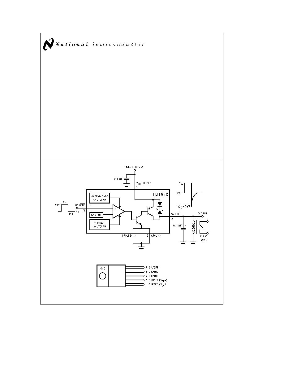
Typical Application
TL H 11237 ≠ 1
Required for stability
Connection Diagram
TO 220 5 Lead
TL H 11237 ≠ 2
Front View
Order Number LM1950T
See NS Package Number T05A
C1995 National Semiconductor Corporation
RRD-B30M115 Printed in U S A
Absolute Maximum Ratings
(Note 1)
If Military Aerospace specified devices are required
please contact the National Semiconductor Sales
Office Distributors for availability and specifications
Supply Voltage
Continuous
26V
Transient (
u
s
100 ms)
b
50V to
a
60V
Reverse Polarity (continuous)
b
15V
On Off Voltage
b
0 3V to
a
6 0V
Power Dissipation
Internally Limited
Load Inductance
150 mH
Maximum Junction Temperature
150 C
Storage Temperature Range
b
65 C to
a
150 C
Lead Temperature
(Soldering 10 seconds)
230 C
ESD Susceptibility (Note 2)
2000V
Operating Ratings
(Note 1)
Temperature Range (T
A
)
b
40 C to
a
125 C
Supply Voltage Range
4 75V to 26V
Thermal Resistances
Junction to Case (i
j-c
)
3 C W
Case to Ambient (i
c-a
)
50 C W
Electrical Characteristics
V
CC
e
14V I
OUT
e
150 mA unless otherwise indicated Boldface limits apply over the entire operating temperature range
b
40 C
s
T
A
s
125 C all other specifications are for T
A
e
T
J
e
25 C
Parameter
Conditions
Typical
Limit
Units
(Limit)
Supply Voltage
Operational
4 75 4 75
V (Min)
26 26
V (Max)
Survival
b
15
b
15
V
DC
(Min)
Transient
t
e
1 ms
u
e
100 ms
60 60
V (Max)
1% dutycycle
b
50
b
50
V (Min)
Supply Current
V
ON OFF
e
0 8V
20
100 100
m
A(Max)
V
ON OFF
e
2 0V
I
OUT
e
0 mA
5
10 10
mA (Max)
I
OUT
e
250 mA
275
350 350
mA (Max)
I
OUT
e
500 mA
550
700 700
mA (Max)
I
OUT
e
750 mA
825
950 950
mA (Max)
Input to Output
I
OUT
e
250 mA
0 30
0 5 0 6
V (Max)
Voltage Drop
I
OUT
e
500 mA
0 50
0 7 1 0
V (Max)
I
OUT
e
750 mA
0 75
1 1 1 4
V (Max)
Short Circuit Current
1 5
1 0 0 75
A (Min)
2 0 2 0
A (Max)
Output Leakage Current
V
ON OFF
e
0 8V
10
50 50
m
A (Max)
ON OFF Input
1 4
0 8 0 8
V (Min)
Threshold Voltage
2 0 2 0
V (Max)
ON OFF Input Current
V
ON OFF
e
0 8V
0 1
5 10
m
A (Max)
V
ON OFF
e
2 0V
1
10 20
m
A (Max)
V
ON OFF
e
5 25V
50
100 100
m
A (Max)
Overvoltage Shutdown
33
27 27
V (Min)
Threshold
37 37
V (Max)
Inductive Clamp
V
ON OFF
e
2V to 0 8V
b
45
b
120
b
120
V (Max)
Output Voltage
I
OUT
e
100 mA
b
40
b
40
V (Min)
Output Turn-On Delay
V
ON OFF
0 8V to 2V
4 2
20
m
s
Output Turn-Off Delay
V
ON OFF
2V to 0 8V
4 5
20
m
s
Note 1
Absolute Maximum Ratings indicate limits beyond which damage to the device may occur Operating Ratings indicate conditions for which the device is
intended to be functional but do not guarantee specific performance limits For guaranteed specifications and test conditions see the Electrical Characteristics
Note 2
Human body model 100 pF discharged through a 1 5 kX resistor
2
Typical Performance Characteristics
Output Voltage vs V
CC
vs Temperature
Output Voltage Drop
vs Output Current
Output Voltage Drop
Peak Output Current
vs Load Current
Operating Current
Dissipation
Maximum Power
vs ON OFF Input Voltage
ON OFF Input Current
vs Temperature
ON OFF Input Current
Voltage vs Supply Voltage
On OFF Input Threshold
TL H 11237 ≠ 3
Turn-On Delay Time
vs Temperature
TL H 11237 ≠ 11
Turn-Off Delay Time
vs Temperature
TL H 11237 ≠ 12
Delay Time Definitions
TL H 11237 ≠ 10
3
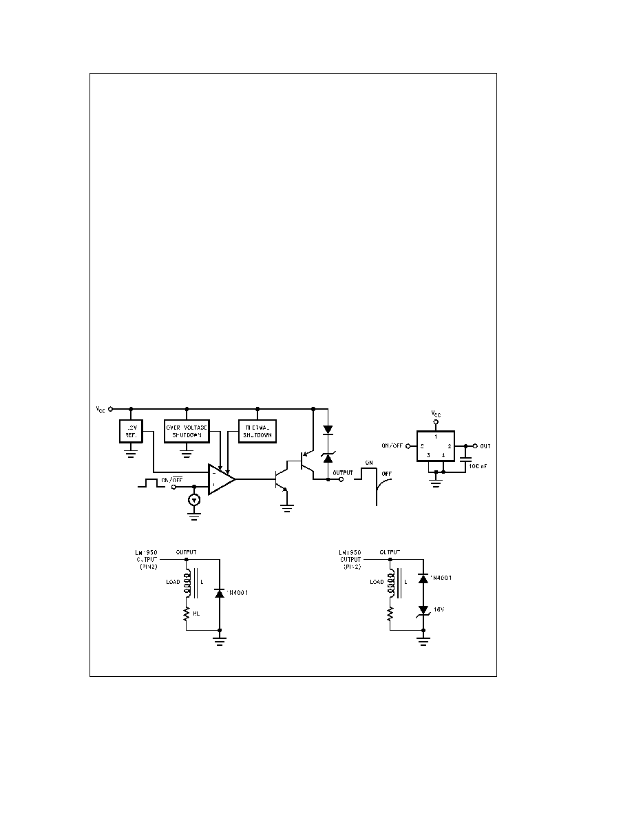
Application Hints
HIGH CURRENT OUTPUT
The 750 mA output is fault protected against overvoltage If
the supply voltage rises above approximately 30V the out-
put will automatically shut down This protects the internal
circuitry and enables the IC to survive higher voltage tran-
sients than would otherwise be expected The LM1950 will
survive transients and DC voltages up to 60V on the supply
The output remains off during this time independent of the
state of the input logic voltage This protects the load The
high current output is also protected against short circuits to
either ground or supply voltage Standard thermal shutdown
circuits are employed to protect the LM1950 from over heat-
ing
FLYBACK RESPONSE
Since the LM1950 is designed to drive inductive as well as
any other type of load inductive kickback can be expected
whenever the output changes state from ON to OFF (See
Waveform on
Figure 1 ) The driver output was left un-
clamped since it is often desirable in many systems to
achieve a very rapid decay in the load current In applica-
tions where this is not true such as in
Figure 2 a simple
external diode clamp will suffice In this application the inte-
grated current in the inductive load is controlled by varying
the duty cycle of the input to the drive IC This technique
achieves response characteristics that are desirable for cer-
tain automotive transmission solenoids for example
For applications requiring a rapid controlled decay in the
solenoid current such as fuel injector drivers an external
zener and diode can be used as in
Figure 3 The voltage
rating of the zener should be such that it breaks down be-
fore the output of the LM1950 The minimum output break-
down voltage of the IC output is rated at
b
54V with respect
to the supply voltage
The LM1950 can be used alone as a simple relay or sole-
noid driver where a rapid decay of the load current is de-
sired but the exact rate of decay is not critical to the sys-
tem If the output is unclamped as in
Figure 1 and the load
is inductive enough the negative flyback transient will cause
the output of the IC to breakdown and behave similarly to a
zener clamp Relying upon the IC breakdown is practical
and will not damage or degrade the IC in any way There are
two considerations that must be accounted for when the
driver is operated in this mode The IC breakdown voltage is
process and lot dependent Output clamp voltages ranging
from
b
40V to
b
120V (with V
CC
supply of 14V) will be en-
countered over time on different devices This is not at all
critical in most applications An important consideration
however is the additional heat dissipated in the IC as a
result This must be added to normal device dissipation
when considering junction temperatures and heat sinking
requirements Worst case for the additional dissipation can
be approximated as
Additional P
D
e
I
2
x L x f(Watts)
Where I
e
Peak Solenoid Current (Amps)
L
e
Solenoid Inductance (Henries)
f
e
Maximum Frequency Input Signal (Hz)
For solenoids where the inductance is less than ten milli-
henries the additional power dissipation can be ignored
Overshoot undershoot and ringing can occur on certain
loads The simple solution is to lower the Q of the load by
the addition of a resistor in parallel or series with the load A
value that draws one tenth of the current or DC voltage of
the load is usually sufficient
For frequency stability of the switch a 0 1 mF or larger out-
put bypass capacitor is required
TL H 11237 ≠ 4
FIGURE 1
TL H 11237 ≠ 5
FIGURE 2 Diode Clamp
TL H 11237 ≠ 6
FIGURE 3 Zener Clamp for Rapid
Controlled Current Decay
4
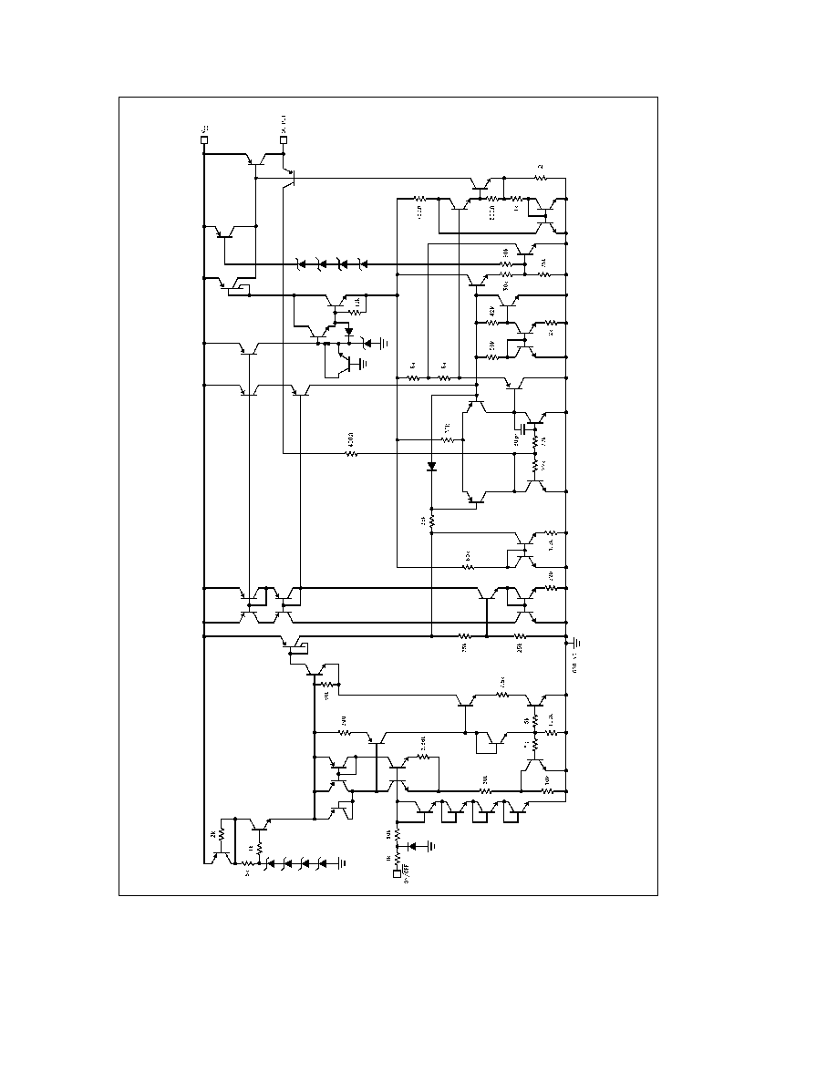
Circuit Schematic
TLH11237
≠
9
5