
TL H 9059
LM196LM396
10
Amp
Adjustable
Voltage
Regulator
August 1992
LM196 LM396 10 Amp Adjustable Voltage Regulator
General Description
The LM196 is a 10 amp regulator adjustable from 1 25V to
15V which uses a revolutionary new IC fabrication structure
to combine high power discrete transistor technology with
modern monolithic linear IC processing This combination
yields a high-performance single-chip regulator capable of
supplying in excess of 10 amps and operating at power lev-
els up to 70 watts The regulators feature on-chip trimming
of reference voltage to
g
0 8% and simultaneous trimming
of reference temperature drift to 30 ppm C typical Thermal
interaction between control circuitry and the pass transistor
which affects the output voltage has been reduced to ex-
tremely low levels by strict attention to isothermal layout
This interaction called thermal regulation is 100% tested
These new regulators have all the protection features of
popular lower power adjustable regulators such as LM117
and LM138 including current limiting and thermal limiting
The combination of these features makes the LM196 im-
mune to blowout from output overloads or shorts even if
the adjustment pin is accidentally disconnected All devices
are ``burned-in'' in thermal shutdown to guarantee proper
operation of these protective features under actual overload
conditions
Output voltage is continuously adjustable from 1 25V to
15V Higher output voltages are possible if the maximum
input-output voltage differential specification is not exceed-
ed Full load current of 10A is available at all output volt-
ages subject only to the maximum power limit of 70W and
of course maximum junction temperature
The LM196 is exceptionally easy to use Only two external
resistors are used to to set output voltage On-chip adjust-
ment of the reference voltage allows a much tighter specifi-
cation of output voltage eliminating any need for trimming in
most cases The regulator will tolerate an extremely wide
range of reactive loads and does not depend on external
capacitors for frequency stabilization Heat sink require-
ments are much less stringent because overload situations
do not have to be accounted for
only worst-case full load
conditions
The LM196 is in a TO-3 package with oversized (0 060 )
leads to provide best possible load regulation Operating
junction temperature range is
b
55 C to
a
150 C The
LM396 is specified for a 0 C to
a
125 C junction tempera-
ture range
Features
Y
Output pre-trimmed to
g
0 8%
Y
10A guaranteed output current
Y
P
a
Product Enhancement tested
Y
70W maximum power dissipation
Y
Adjustable output
1 25V to 15V
Y
Internal current and power limiting
Y
Guaranteed thermal resistance
Y
Output voltage guaranteed under worst-case conditions
Y
Output is short circuit protected
Typical Applications
V
OUT
e
(1 25V)
R1
a
R2
R1
J
a
I
ADJ
(R2)
TL H 9059 � 1
For best TC of V
OUT
R1 should be wirewound
or metal film 1% or better
R2 should be same type as R1 with TC track-
ing of 30 ppm C or better
C1 is necessary only if main filter capacitor is
more than 6
away assuming
18 or larger
leads
C2 is not absolutely necessary but is suggest-
ed to lower high frequency output impedance
Output capacitors in the range of 1 mF to
1000 mF of aluminum or tantalum electrolytic
are commonly used to provide improved out-
put impedance and rejection of transients
C3 improves ripple rejection output imped-
ance and noise C2 should be 1 mF or larger
close to the regulator if C3 is used
FIGURE 1 Basic 1 25V to 15V Regulator
C1995 National Semiconductor Corporation
RRD-B30M115 Printed in U S A

Absolute Maximum Ratings
If Military Aerospace specified devices are required
please contact the National Semiconductor Sales
Office Distributors for availability and specifications
Power Dissipation
Internally Limited
Input-Output Voltage Differential
20V
Operating Junction Temperature Range
LM196 Control Section
b
55 C to
a
150 C
Power Transistor
b
55 C to
a
200 C
LM396 Control Section
0 C to
a
125 C
Power Transistor
0 C to
a
175 C
Storage Temperature
b
65 C to
a
150 C
Lead Temperature (Soldering 10 seconds)
300 C
ESD rating to be determined
Electrical Characteristics
(Note 1)
Parameter
Conditions
LM196
LM396
Units
Min
Typ
Max
Min
Typ
Max
Reference Voltage
I
OUT
e
10 mA
1 24
1 25
1 26
1 23
1 25
1 27
V
Reference Voltage
V
MIN
s
(V
IN
b
V
OUT
)
s
20V
1 22
1 25
1 28
1 21
1 25
1 29
V
(Note 2)
10 mA
s
I
OUT
10A P
s
P
MAX
Full Temperature Range
Line Regulation
V
MIN
s
(V
IN
b
V
OUT
)
s
20V
0 005
0 01
0 005
0 02
% V
(Note 3)
Full Temperature Range
0 05
0 05
% V
Load Regulation
10 mA
s
I
OUT
s
10A
0 1
0 1
% A
LM196 LM396
V
MIN
s
V
IN
b
V
OUT
s
10V P
s
P
MAX
(Note 4)
Full Temperature Range
0 15
0 15
% A
Ripple Rejection
C
ADJ
e
25 mF f
e
120 Hz
60
74
66
74
dB
(Note 5)
Full Temperature Range
54
54
dB
Thermal Regulation
V
IN
b
V
OUT
e
5V I
OUT
e
10A
0 003
0 005
0 003
0 015
% W
(Note 6)
Average Output Voltage
T
jMIN
s
T
j
s
T
jMAX
0 003
0 003
% C
Temperature Coefficient
(See Curves for Limits)
Adjustment Pin Current
50
100
50
100
m
A
Adjustment Pin Current
10 mA
s
I
OUT
s
10A
3
3
m
A
Change (Note 7)
3V
s
V
IN
b
V
OUT
s
20V
P
s
P
MAX
Full Temperature Range
Minimum Load Current
2 5V
s
(V
IN
b
V
OUT
)
s
20V
10
10
mA
(Note 9)
Full Temperature Range
Current Limit
2 5
s
(V
IN
b
V
OUT
s
7V
10
14
20
10
14
20
A
(Note 8)
V
IN
b
V
OUT
e
20V
1 5
3
8
1 5
3
8
A
Rms Output Noise
10 Hz
s
f
s
10 kHz
0 001
0 001
%V
OUT
Long Term Stability
T
j
e
125 C t
e
1000 Hours
0 3
1 0
0 3
1 0
%
Thermal Resistance
Control Circuitry
0 3
0 5
0 3
0 5
C W
Junction to Case
Power Transistor
1 0
1 2
1 0
1 2
C W
(Note 10)
2

Electrical Characteristics
(Note 1) (Continued)
Parameter
Conditions
LM196
LM396
Units
Min
Typ
Max
Min
Typ
Max
Power Dissipation (P
MAX
)
7 0V
s
V
IN
b
V
OUT
s
12V
70
100
70
100
W
(Note 11)
V
IN
b
V
OUT
e
15V
50
50
W
V
IN
b
V
OUT
e
18V
36
36
W
Drop-Out Voltage
I
OUT
e
10A
2 1
2 5
2 1
2 5
V
LM196 LM396
Full Temperature Range
2 75
2 75
Note 1
Unless otherwise stated these specifications apply for T
j
e
25 C V
IN
b
V
OUT
e
5V I
OUT
e
10 mA to 10A
Note 2
This is a worst-case specification which includes all effects due to input voltage output current temperature and power dissipation Maximum power
(P
MAX
) is specified under Electrical Characteristics
Note 3
Line regulation is measured on a short-pulse low-duty-cycle basis to maintain constant junction temperature Changes in output voltage due to thermal
gradients or temperature changes must be taken into account separately See discussion of Line Regulation under Application Hints
Note 4
Load regulation on the 2-pin package is determined primarily by the voltage drop along the output pin Specifications apply for an external Kelvin sense
connnection at a point on the output pin
from the bottom of the package Testing is done on a short-pulse-width low-duty-cycle basis to maintain constant
junction temperature Changes in output voltage due to thermal gradients or temperature changes must be taken into account separately See discussion of Load
Regulation under Application Hints
Note 5
Ripple rejection is measured with the adjustment pin bypassed with 25 mF capacitor and is therefore independent of output voltage With no load or
bypass capacitor ripple rejection is determined by line regulation and may be calculated from RR
e
20 log
10
100 (K
c
V
OUT
) where K is line regulation
expressed in % V At frequencies below 100 Hz ripple rejection may be limited by thermal effects if load current is above 1A
Note 6
Thermal regulation is defined as the change in output voltage during the time period of 0 2 ms to 20 ms after a change in power dissipation in the regulator
due to either a change in input voltage or output current See graphs and discussion of thermal effects under Application Hints
Note 7
Adjustment pin current change is specified for the worst-case combination of input voltage output current and power dissipation Changes due to
temperature must be taken into account separately See graph of adjustment pin current vs temperature
Note 8
Current limit is measured 10 ms after a short is applied to the output DC measurements may differ slightly due to the rapidly changing junction temperature
tending to drop slightly as temperature increases A minimum available load current of 10A is guaranteed over the full temperature range as long as power
dissipation does not exceed 70W and V
IN
b
V
OUT
is less than 7 0V
Note 9
Minimum load current of 10 mA is normally satisfied by the resistor divider which sets up output voltage
Note 10
Total thermal resistance junction-to-ambient will include junction-to-case thermal resistance plus interface resistance and heat sink resistance See
discussion of Heat Sinking under Application Hints
Note 11
Although power dissipation is internally limited electrical specifications apply only for power dissipation up to the limits shown Derating with temperature
is a function of both power transistor temperature and control area temperature which are specified differently See discussion of Heat Sinking under Application
Hints For V
IN
b
V
OUT
less than 7V power dissipation is limited by current limit of 10A
Note 12
Dropout voltage is input-output voltage differential measured at a forced reference voltage of 1 15V with a 10A load and is a measurement of the
minimum input output differential at full load
Application Hints
Further improvements in efficiency can be obtained by using
Schottky diodes or high efficiency diodes with lower forward
voltage combined with larger filter capacitors to reduce rip-
ple However this reduces the voltage difference between
input and drive pins and may not allow sufficient voltage to
fully saturate the pass transistor Special transformers are
available from Signal Transformer that have a 1V tap on the
output winding to provide the extra voltage for the drive pin
The transformers are available as standard items for 5V ap-
plications at 5A 10A and 20A Other voltages are available
on special request
Heat Sinking
Because of its extremely high power dissipation capability
the
major limitation in the load driving capability of the
LM196 is
heat sinking Previous regulators such as LM109
LM340 LM117 etc
had internal power limiting circuitry
which limited power dissipation to about 30W The LM196
is guaranteed to dissipate up to 70W continuously as long
as the maximum junction temperature limit is not exceeded
This requires careful attention to all sources of thermal re-
sistance from junction-to-ambient
including junction-to-
case resistance
case-to-heat sink interface resistance
(0 1 � 1 0 C W) and heat sink resistance itself A good ther-
mal joint compound such as Wakefield type 120 or Thermal-
loy Thermocote must be used when mounting the LM196
especially if an electrical insulator is used to isolate the reg-
ulator from the heat sink Interface resistance without this
compound will be no better than 0 5 C W and probably
much worse With the compound and no insulator interface
resistance will be 0 2 C W or less assuming 0 005 or less
combined flatness run-out of TO-3 and heat sink Proper
torquing of the mounting bolts is important to achieve mini-
mum thermal resistance Four to six inch pounds is recom-
mended Keep in mind that good electrical as well as ther-
mal contact must be made to the case
3

Application Hints
(Continued)
The actual heat sink chosen for the LM196 will be deter-
mined by the worst-case continuous full load current input
voltage and maximum ambient temperature Overload or
short circuit output conditions do not normally have to be
considered when selecting a heat sink because the thermal
shutdown built into the LM196 will protect it under these
conditions An exception to this is in situations where the
regulator must recover very quickly from overload The
LM196 may take some time to recover to within specified
output tolerance following an extended overload if the regu-
lator is cooling from thermal shutdown temperature (approx-
imately 175 ) to specified operating temperature (125 C or
150 C) The procedure for heat sink selection is as follows
Calculate worst-case
continuous average power dissipa-
tion in the regulator from P
e
(V
IN
b
V
OUT
)
c
(I
OUT
) To
do this you must know the raw power supply voltage cur-
rent characteristics fairly accurately For example consid-
er a 10V output with 15V nominal input voltage At full
load of 10A the regulator will dissipate P
e
(15
b
10)
c
(10)
e
50W If input voltage rises by 10% power dissipa-
tion will increase to (16 5
b
10)
c
(10)
e
65W a
30%
increase It is strongly suggested that a raw supply be
assembled and tested to determine its average DC output
voltage
under full load with maximum line voltage Do not
over-design by using unloaded voltage as a worst-case
since the regulator will not be dissipating any power under
no load conditions Worst-case regulator dissipation nor-
mally occurs under full load conditions except when the
effective DC resistance of the raw supply (DV DI) is larg-
er than (V
IN
b
V
OUT
) 2I
fL
where V
IN
is the lightly-load-
ed raw supply voltage and I
fL
is full load current For (V
IN
b
V
OUT
)
e
5V
b
8V and I
fL
e
5A � 10A this gives a
resistance of 0 25X to 0 8X If raw supply resistance is
higher than this the regulator power dissipation may be
less at full load current then at some intermediate cur-
rent due to the large drop in input voltage Fortunately
most well designed raw supplies have low enough output
resistance that regulator dissipation does maximize at full
load current or very close to it so tedious testing is not
usually required to find worst-case power dissipation
A very important consideration is the size of the filter capac-
itor in the raw supply At these high current levels capacitor
size is usually dictated by ripple current ratings rather than
just obtaining a certain ripple voltage Capacitor ripple cur-
rent (rms) is 2 � 3 times the DC output current of the filter If
the capacitor has just 0 05X DC resistance this can cause
30W internal power dissipation at 10A output current Ca-
pacitor life is very sensitive to operating temperature de-
creasing by a factor of two for each 15 C rise in internal
temperature Since capacitor life is not all that great to start
with it is obvious that a small capacitor with a large internal
temperature rise is inviting very short mean-time-to-failure
A second consideration is the loss of usable input voltage to
the regulator If the capacitor is small the large dips in the
input voltage may cause the LM196 to drop out of regula-
tion 2000 mF per ampere of load current is the
minimum
recommended value yielding about 2 Vp-p ripple of 120 Hz
Larger values will have longer life and the reduced ripple will
allow lower DC input voltage to the regulator with subse-
quent cost savings in the transformer and heat sink Some-
times several capacitors in parallel are better to decrease
series resistance and increase heat dissipating area
After the raw supply characteristics have been determined
and worst-case power dissipation in the LM196 is known
the heat sink thermal resistance can be found from the
graphs titled Maximum Heat Sink Thermal Resistance
These curves indicate the minimim size heat sink required
as a function of ambient temperature They are derived from
a case-to-control area thermal resistance of 0 5 C W and a
case-to-power transistor thermal resistance of 1 2 C W
0 2 C W is assumed for interface resistance A maximum
control area temperature of 150 C is used for the LM196
and 125 C for the LM396 Maximum power transistor tem-
perature is 200 C for the LM196 and 175 C for the LM396
For conservative designs it is suggested that when using
these curves you assume an ambient temperature 25 C �
50 C higher than is actually anticipated to avoid running the
regulator right at its design limits of operating temperature
A quick look at the curves show that heat sink resistance
(i
SA
) will normally fall into the range of 0 2 C W � 1 5 C W
These are
not small heat sinks A model 441 for instance
which is sold by several manufacturers has a i
SA
of
0 6 C W with natural convection and is about five inches on
a side Smaller sinks are more volumetrically efficient and
larger sinks less so A rough formula for estimating the vol-
ume of heat sink required is V
e
50 i
SA
1 5
CU IN This
holds for natural convection only If the heat sink is inside a
small sealed enclosure i
SA
will increase substantially be-
cause the air is not free to form natural convection currents
Fan-forced convection can reduce i
SA
by a factor of two at
200 FPM air velocity and by four at 1000 FPM
Ripple Rejection
Ripple rejection at the normal ripple frequency of 120 Hz is
a function of both electrical and thermal effects in the
LM196 If the adjustment pin is not bypassed with a capaci-
tor it is also dependent on output voltage A 25 mF capaci-
tor from the adjustment pin to ground will make ripple rejec-
tion independent of output voltage for frequencies above
100 Hz If lower ripple frequencies are encountered the ca-
pacitor should be increased proportionally
To keep in mind that the bypass capacitor on the adjust-
ment pin will limit the turn-on time of the regulator A 25 mF
capacitor combined with the output divider resistance will
give an extended output voltage settling time following the
application of input power
Load Regulation (LM196 LM396)
Because the LM196 is a three-terminal device it is not pos-
sible to provide true remote load sensing Load regulation
will be limited by the resistance of the output pin and the
wire connecting the regulator to the load For the data sheet
specification regulation is measured 1 4
from the bottom
of the package on the output pin Negative side sensing is a
true Kelvin connection with the bottom of the output divider
returned to the negative side of the load
4
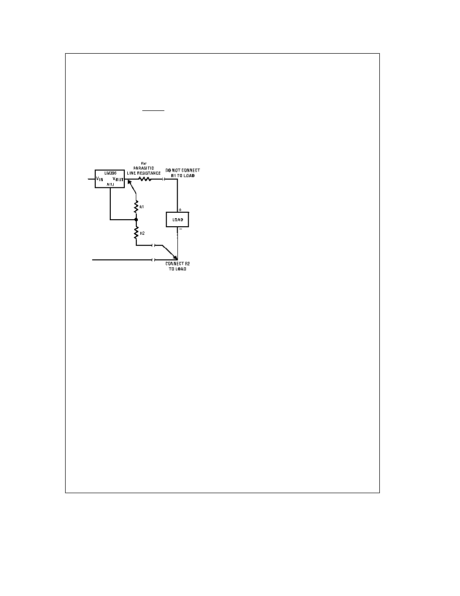
Application Hints
(Continued)
Although it may not be immediately obvious best load regu-
lation is obtained when the top of the divider is connected
directly to the output pin not to the load This is illustrated in
Figure 2 If R1 were connected to the load the effective
resistance between the regulator and the load would be
(Rw)
c
R2
a
R1
R1
J
Rw
e
Line Resistance
Connected as shown Rw is not multiplied by the divider
ratio Rw is about 0 004X per foot using 16 gauge wire This
translates to 40 mV ft at 10A load current so it is important
to keep the positive lead between regulator and load as
short as possible
TL H 9059 � 2
FIGURE 2 Proper Divider Connection
The input resistance of the sense pin is typically 6 kX mod-
eled as a resistor between the sense pin and the output pin
Load regulation will start to degrade if a resistance higher
than 10X is inserted in series with the sense This assumes
a worst-case condition of 0 5V between output and sense
pins Lower differential voltage will allow higher sense series
resistance
Thermal Load Regulation
Thermal as well as electrical load regulation must be con-
sidered with IC regulators Electrical load regulation occurs
in microseconds thermal regulation due to die thermal gra-
dients occurs in the 0 2 ms-20 ms time frame and regula-
tion due to overall temperature changes in the die occurs
over a 20 ms to 20 minute period depending on the time
constant of the heat sink used Gradient induced load regu-
lation is calculated from
D
V
OUT
e
(V
IN
b
V
OUT
)
c
(DI
OUT
)
c
(b)
b
e
Thermal regulation specified on data sheet
For V
IN
e
9V V
OUT
e
5V DI
OUT
e
10A and b
e
0 005% W this yields a 0 2% change in output voltage
Changes in output voltage due to overall temperature rise
are calculated from
V
OUT
e
(V
IN
b
V
OUT
)
c
(DI
OUT
)
c
(TC)
c
(i
jA
)
TC
e
Temperature coefficient of output voltage
i
jA
e
Thermal resistance from junction to ambient i
jA
is
approximately 0 5 C W
a
i
of heat sink
For the same conditions as before with TC
e
0 003% C
and i
jA
e
1 5 C W the change in output voltage will be
0 18% Because these two thermal terms can have either
polarity they may subtract from or add to electrical load
regulation For worst-case analysis they must be assumed
to add If the output of the regulator is trimmed under load
only that portion of the load that changes need be used in
the previous calculations significantly improving output ac-
curacy
Line Regulation
Electrical line regulation is very good on the LM196
typi-
cally less than 0 005% change in output voltage for a 1V
change in input This level of regulation is achieved only for
very low load currents however because of thermal ef-
fects Even with a thermal regulation of 0 002% W and a
temperature coefficient of 0 003% C DC line regulation
will be dominated by thermal effects as shown by the follow-
ing example
Assume V
OUT
e
5V V
IN
e
9V I
OUT
e
8A
Following a 10% change in input voltage (0 9) the output
will change quickly (
s
100 ms) due to electrical effects by
(0 005%V)
c
(0 9V)
e
0 0045% In the next 20 ms the
output will change an additional (0 002% W)
c
(8A)
c
(0 9V)
e
0 0144% due to thermal gradients across the die
After a much longer time determined by the time constant
of the heat sink the output will change an additional
(0 003% C)
c
(8A)
c
(0 9V)
c
(2 C W)
e
0 043% due to
the temperature coefficient of output voltage and the ther-
mal resistance from die to ambient (2 C W was chosen for
this calculation) The sign of these last two terms varies
from part to part so no assumptions can be made about any
cancelling effects All three terms must be added for a prop-
er analysis This yields 0 0045
a
0 0144
a
0 043
e
0 062% using
typical values for thermal regulation and tem-
perature coefficient For worst-case analysis the maximum
data sheet specifications for thermal regulation and temper-
ature coefficient should be used along with the
actual ther-
mal resistance of the heat sink being used
Paralleling Regulators
Direct paralleling of regulators is not normally recommend-
ed because they do not share currents equally The regula-
tor with the highest reference voltage will supply all the cur-
rent to the load until it current limits With an 18A load for
instance one regulator might be operating in current limit at
16A while the second device is only carrying 2A Power dis-
sipation in the high current regulator is extremely high with
attendant high junction temperatures Long term reliability
cannot be guaranteed under these conditions
Quasi-paralleling may be accomplished if load regulation is
not critical The connection shown in
Figure 5a will typically
share to within 1A with a worst-case of about 3A Load
regulation is degraded by 150 mV at 20A loads An external
op amp may be used as in
Figure 5b to improve load regula-
tion and provide remote sensing
5