LM1971Overture
TM
Audio Attenuator Series
Digitally Controlled 62 dB Audio Attenuator with/Mute
General Description
The LM1971 is a digitally controlled single channel audio
attenuator fabricated on a CMOS process. Attenuation is
variable in 1 dB steps from 0 dB to -62 dB. A mute function
disconnects the input from the output, providing over 100 dB
of attenuation.
The performance of the device is exhibited by its ability to
change attenuation levels without audible clicks or pops. In
addition, the LM1971 features a low Total Harmonic Distor-
tion (THD) of 0.0008%, and a Dynamic Range of 115 dB,
making it suitable for digital audio needs. The LM1971 is
available in both 8-pin plastic DIP or SO packages.
The LM1971 is controlled by a TTL/CMOS compatible 3-wire
serial digital interface. The active low LOAD line enables the
data input registers while the CLOCK line provides system
timing. Its DATA pin receives serial data on the rising edge of
each CLOCK pulse, allowing the desired attenuation setting
to be selected.
Key Specifications
n
Total harmonic distortion
0.0008% (typ)
n
Frequency response
>
200 kHz (-3 dB) (typ)
n
Attenuation range (excluding mute)
62 dB (typ)
n
Dynamic range
115 dB (typ)
n
Mute attenuation
102 dB (typ)
Features
n
3-wire serial interface
n
Mute function
n
Click and pop free attenuation changes
n
8-pin plastic DIP and SO packages available
Applications
n
Communication systems
n
Cellular Phones and Pagers
n
Personal computer audio control
n
Electronic music (MIDI)
n
Sound reinforcement systems
n
Audio mixing automation
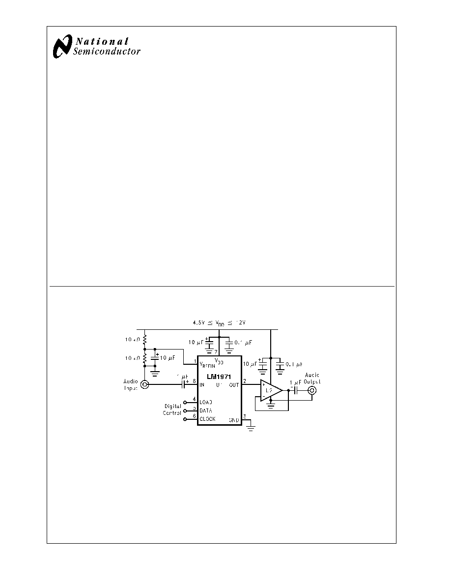
Typical Application
Overture
TM
is a trademark of National Semiconductor Corporation.
01235301
FIGURE 1. Typical Audio Attenuator Application Circuit
September 2002
LM1971
Overture
Audio
Attenuator
Series
Digitally
Controlled
62
dB
Audio
Attenuator
with
Mute
� 2002 National Semiconductor Corporation
DS012353
www.national.com
Absolute Maximum Ratings
(Notes 1,
2)
If Military/Aerospace specified devices are required,
please contact the National Semiconductor Sales Office/
Distributors for availability and specifications.
Supply Voltage, V
DD
15V
Voltage at any pin
(GND -0.2V) to (V
DD
+0.2V)
ESD Susceptibility (Note 4)
3000V
Soldering Information
N Package (10s)
M Package
Vapor Phase (60s)
Infrared (15s)
260�C
215�C
220�C
Power Dissipation (Note 3)
150 mW
Junction Temperature
150�C
Storage Temperature
-65�C to +150�C
Operating Ratings
(Notes 1, 2)
Temperature Range
T
MIN
T
A
T
MAX
-40�C
T
A
+85�C
Thermal Resistance
M08A Package,
JA
167�C/W
N08E Package,
JA
102�C/W
Supply Voltage
4.5V to 12V
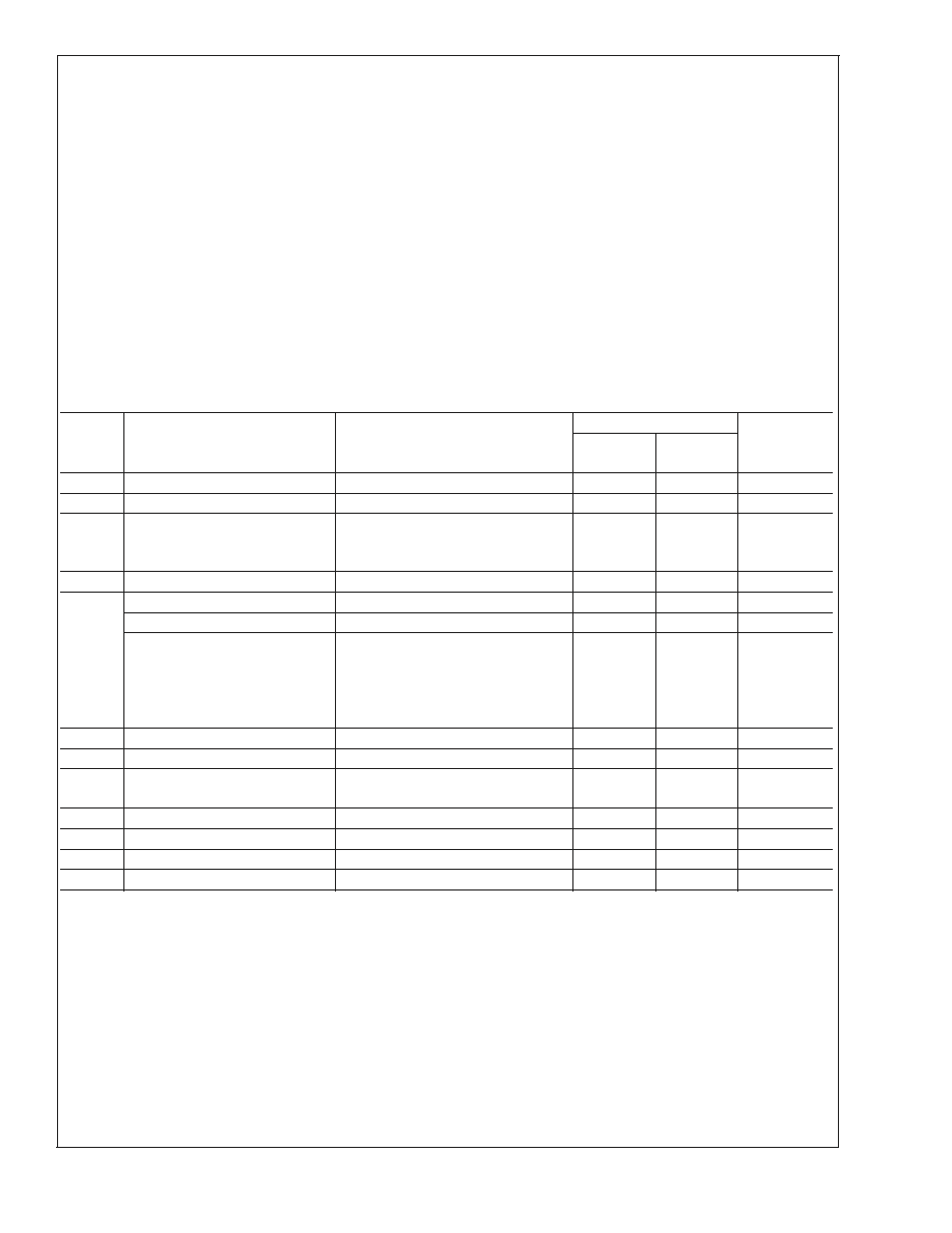
Electrical Characteristics
(Notes 1, 2)
The following specifications apply for V
DD
= +12V (V
REF
IN = +6V), V
IN
= 5.5 V
pk
, and f = 1 kHz, unless otherwse specified.
Limits apply for T
A
= 25�C. Digital inputs are TTL and CMOS compatible.
Symbol
Parameter
Conditions
LM1971
Units
(Limits)
Typical
(Note 5)
Limit
(Note 6)
I
S
Supply Current
Digital Inputs Tied to 6V
1.8
3
mA (max)
THD
Total Harmonic Distortion
V
IN
= 0.5V
pk
@
0 dB Attenuation
0.0008
0.003
% (max)
e
IN
Noise
Input is AC Grounded
@
-12 dB Attenuation
A-Weighted (Note 7)
4.0
�V
DR
Dynamic Range
Referenced to Full Scale = +6 V
pk
115
dB
A
M
Mute Attenuation
102
96
dB (min)
Attenuation Step Size Error
0 dB to -62 dB
0.009
0.2
dB (max)
Absolute Attenuation
Attenuation
@
0 dB
Attenuation
@
-20 dB
Attenuation
@
-40 dB
Attenuation
@
-60 dB
Attenuation
@
-62 dB
0.1
-20.3
-40.5
-60.6
-62.6
0.5
-19.0
-38.0
-57.0
-59.0
dB (min)
dB (min)
dB (min)
dB (min)
dB (min)
I
LEAK
Analog Input Leakage Current
Input is AC Grounded
5.8
100
nA (max)
Frequency Response
20 Hz�100 kHz
�
0.1
dB
R
IN
AC Input Impedance
Pin 8, V
IN
= 1.0 V
pk
, f = 1 kHz
40
20
60
k
(min)
k
(max)
I
IN
Input Current
@
Pins 4, 5, 6
@
0V
<
V
IN
<
5V
1.0
100
nA (max)
f
CLK
Clock Frequency
3
2
MHz (max)
V
IH
High-Level Input Voltage
@
Pins 4, 5, 6
2.0
V (min)
V
IL
Low-Level Input Voltage
@
Pins 4, 5, 6
0.8
V (max)
Note 1: Absolute Maximum Ratings indicate limits beyond which damage to the device may occur. Operating Ratings indicate conditions for which the device is
functional, but do not guarantee specific performance limits. Electrical Characteristics state DC and AC electrical specifications under particular test conditions which
guarantee specific performance limits. This assumes that the device is within the Operating Ratings. Specifications are not guaranteed for parameters where no limit
is given, however, the typical value is a good indication of device performance.
Note 2: All voltages are measured with respect to the GND pin (pin 3), unless otherwise specified.
Note 3: The maximum power dissipation must be derated at elevated temperatures and is dictated by T
JMAX
,
JA
, and the ambient temperature T
A
. The maximum
allowable power dissipation is P
D
= (T
JMAX
� T
A
)/
JA
or the number given in the Absolute Maximum Ratings, whichever is lower. For the LM1971N and LM1971M,
T
JMAX
= +150�C, and the typical junction-to-ambient thermal resistance,
JA
, when board mounted is 102� C/W and 167� C/W, respectively.
Note 4: Human body model, 100 pF discharged through a 1.5 k
resistor.
Note 5: Typicals are measured at 25�C and represent the parametric norm.
Note 6: Limits are guarantees that all parts are tested in production to meet the stated values.
Note 7: Due to production test limitations, there is no limit for the Noise test. Please refer to the noise measurements in the Typical Performance Characteristics
section.
LM1971
www.national.com
3
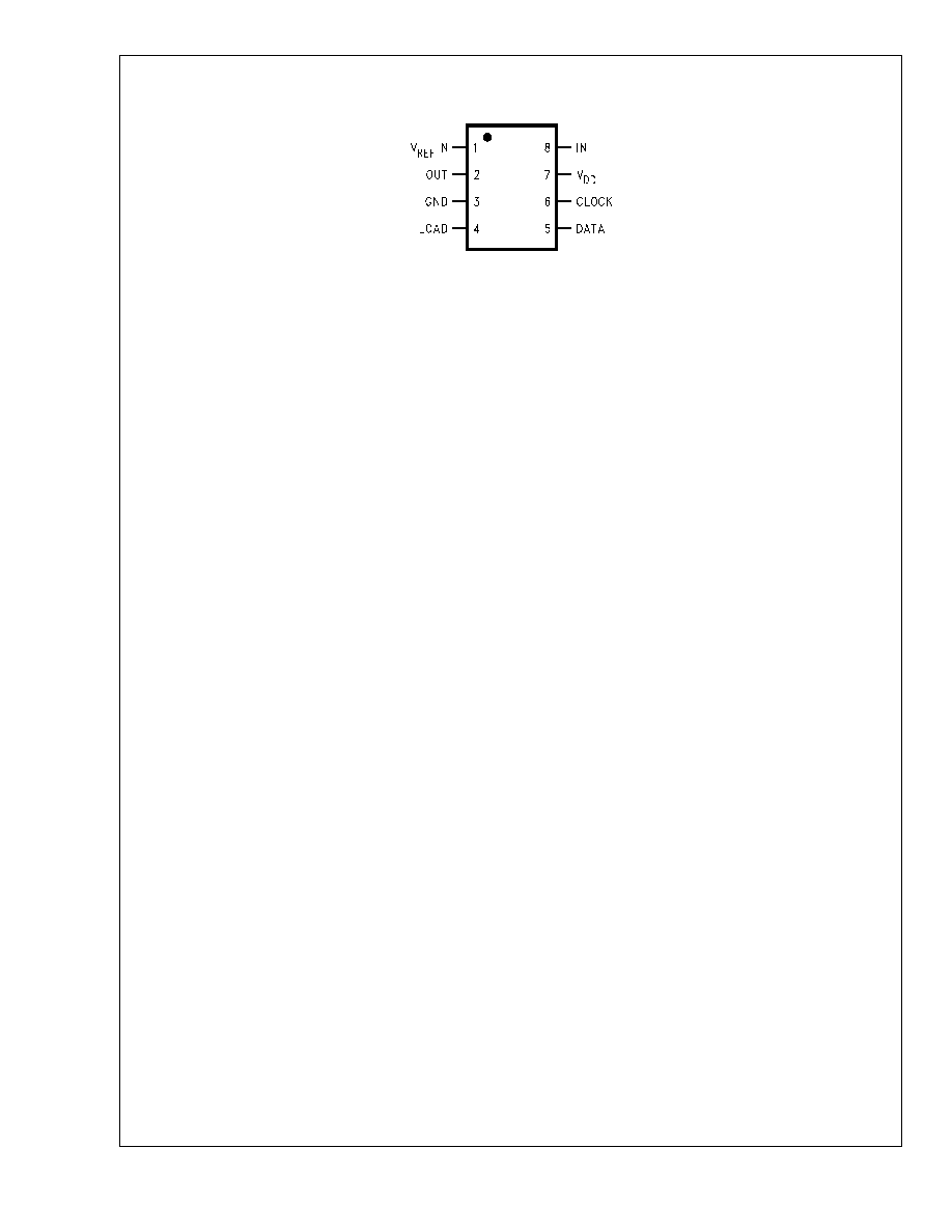
Pin Descriptions
V
REF
IN (1): The V
REF
IN pin provides the reference for the
analog input signal. This pin should be biased at half of the
supply voltage, V
DD
, as shown in Figure 1 and Figure 6.
OUT (2): The attenuated analog output signal comes from
this pin.
GND (3): The GND pin references the digital input signals
and is the lower voltage reference for the IC. Typically this
pin would be labeled "V
SS
" but the ground reference for the
digital logic input control is tied to this same point. With a
higher pin-count there would generally be separate pins for
these functions; V
SS
and Logic Ground. It is intended that
the LM1971 always be operated using a single voltage sup-
ply configuration, for which pin 3 (GND) should always be at
system ground. If a bipolar or split-supply configuration are
desired, level shifting circuitry is needed for the digital logic
control pins as they would be referenced through pin 3 which
would be at the negative supply. It is highly recommended,
however, that the LM1971 be used in a unipolar or
single-supply configuration.
LOAD (4): The LOAD input accepts a TTL or CMOS level
signal. This is the enable pin of the device, allowing data to
be clocked in while this input is low (0V). The GND pin is the
reference for this signal.
DATA (5): The DATA input accepts a TTL or CMOS level
signal. This pin is used to accept serial data from a micro-
controller that will be latched and decoded to change the
channel's attenuation level. The GND pin is the reference for
this signal.
CLOCK (6): The CLOCK input accepts a TTL or CMOS level
signal. The clock input is used to load data into the internal
shift register on the rising edge of the input clock waveform.
The GND pin is the reference for this signal.
V
DD
(7): The positive voltage supply should be placed to this
pin.
IN (8): The analog input signal should be placed to this pin.
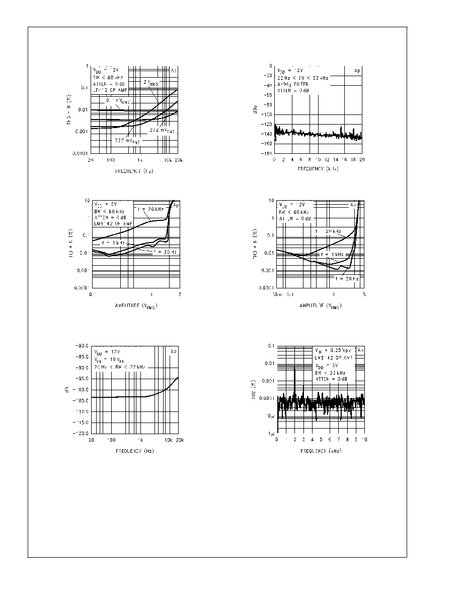
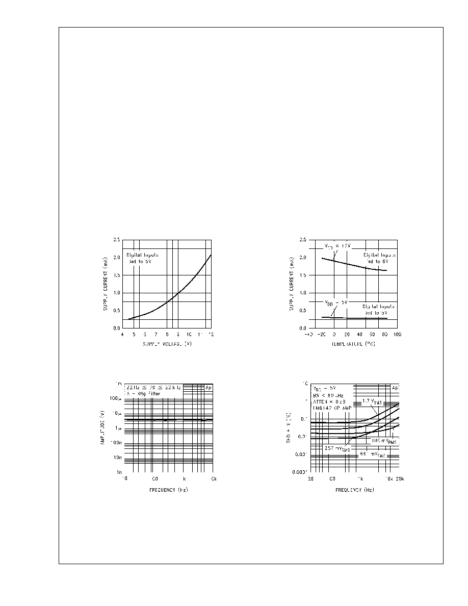
Typical Performance Characteristics
Supply Current vs
Supply Voltage
Supply Current vs
Temperature
01235310
01235311
Noise Floor
Analog Measurement
THD + N vs Freq and Amp
01235312
01235313
LM1971
www.national.com
4