Äîêóìåíòàöèÿ è îïèñàíèÿ www.docs.chipfind.ru

LM20EP
Enhanced Plastic 2.4V, 10µA, SC70, micro SMD
Temperature Sensor
General Description
The LM20EP is a precision analog output CMOS integrated-
circuit temperature sensor that operates over a -55°C to
+130°C temperature range. The power supply operating
range is +2.4 V to +5.5 V. The transfer function of LM20EP is
predominately linear, yet has a slight predictable parabolic
curvature. The accuracy of the LM20EP when specified to a
parabolic transfer function is
±
1.5°C at an ambient tempera-
ture of +30°C. The temperature error increases linearly and
reaches a maximum of
±
2.5°C at the temperature range
extremes. The temperature range is affected by the power
supply voltage. At a power supply voltage of 2.7 V to 5.5 V
the temperature range extremes are +130°C and -55°C.
Decreasing the power supply voltage to 2.4 V changes the
negative extreme to -30°C, while the positive remains at
+130°C.
The LM20EP's quiescent current is less than 10 µA. There-
fore, self-heating is less than 0.02°C in still air. Shutdown
capability for the LM20EP is intrinsic because its inherent
low power consumption allows it to be powered directly from
the output of many logic gates or does not necessitate
shutdown at all.
ENHANCED PLASTIC
·
Extended Temperature Performance of -55°C to +130°C
·
Baseline Control - Single Fab & Assembly Site
·
Process Change Notification (PCN)
·
Qualification & Reliability Data
·
Solder (PbSn) Lead Finish is standard
·
Enhanced Diminishing Manufacturing Sources (DMS)
Support
Features
n
Rated for full -55°C to +130°C range
n
Available in an SC70 and a micro SMD package
n
Predictable curvature error
n
Suitable for remote applications
Key Specifications
j
Accuracy at +30°C
±
1.5 to
±
4 °C (max)
j
Accuracy at +130°C & -55°C
±
2.5 to
±
5 °C (max)
j
Power Supply Voltage Range
+2.4V to +5.5V
j
Current Drain
10 µA (max)
j
Nonlinearity
±
0.4 % (typ)
j
Output Impedance
160
(max)
j
Load Regulation
0 µA
<
I
L
<
+16 µA
-2.5 mV (max)
Applications
n
Battery Management
n
Selected Military Applications
n
Selected Avionics Applications
Ordering Information
PART NUMBER
VID PART NUMBER
NS PACKAGE NUMBER (Note 3)
LM20CIM7EP
V62/04728-01
MAA05A
(Notes 1, 2)
TBD
TBD
Note 1: For the following (Enhanced Plastic) version, check for availability: LM20SIBPEP, LM20SIBPXEP, LM20BIM7EP, LM20BIM7XEP,
LM20CIM7XEP, LM20SITLEP, LM20SITLXEP. Parts listed with an "X" are provided in Tape & Reel and parts without an "X" are in Rails.
Note 2: FOR ADDITIONAL ORDERING AND PRODUCT INFORMATION, PLEASE VISIT THE ENHANCED PLASTIC WEB SITE AT: www.national.com/
mil
Note 3: Refer to package details under Physical Dimensions
May 2004
LM20EP
Enhanced
Plastic
2.4V
,
10µA,
SC70,
micro
SMD
T
emperature
Sensor
© 2004 National Semiconductor Corporation
DS200999
www.national.com
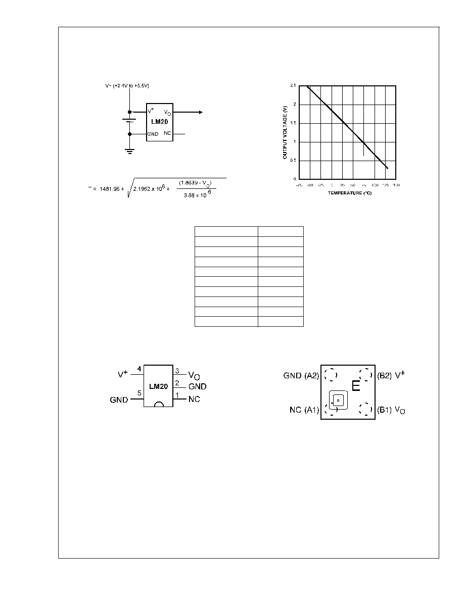
Typical Application
Full-Range Celsius (Centigrade) Temperature Sensor (-55°C to +130°C)
Operating from a Single Li-Ion Battery Cell
Output Voltage vs Temperature
20099902
V
O
= (-3.88x10
-6
xT
2
) + (-1.15x10
-2
xT) + 1.8639
where:
T is temperature, and V
O
is the measured output voltage of the LM20EP.
20099924
Temperature (T)
Typical V
O
+130°C
+303 mV
+100°C
+675 mV
+80°C
+919 mV
+30°C
+1515 mV
+25°C
+1574 mV
0°C
+1863.9 mV
-30°C
+2205 mV
-40°C
+2318 mV
-55°C
+2485 mV
Connection Diagrams
SC70-5
micro SMD
20099901
Note:
-
GND (pin 2) may be grounded or left floating. For optimum thermal
conductivity to the pc board ground plane pin 2 should be grounded.
-
NC (pin 1) should be left floating or grounded. Other signal traces
should not be connected to this pin.
Top View
See NS Package Number MAA05A
20099932
Note:
-
Pin numbers are referenced to the package marking text orientation.
-
Reference JEDEC Registration MO-211, variation BA
-
The actual physical placement of package marking will vary slightly from
part to part. The package marking will designate the date code and will vary
considerably. Package marking does not correlate to device type in any way.
Top View
See NS Package Number BPA04DDC and TLA04ZZA
LM20EP
Enhanced
Plastic
www.national.com
2

Absolute Maximum Ratings
(Note 4)
If Military/Aerospace specified devices are required,
please contact the National Semiconductor Sales Office/
Distributors for availability and specifications.
Supply Voltage
+6.5V to -0.2V
Output Voltage
(V
+
+ 0.6 V) to
-0.6 V
Output Current
10 mA
Input Current at any pin (Note 5)
5 mA
Storage Temperature
-65°C to
+150°C
Maximum Junction Temperature
(T
JMAX
)
+150°C
ESD Susceptibility (Note 6) :
Human Body Model
2500 V
Machine Model
250 V
Lead Temperature
SC-70 Package (Note 7) :
Vapor Phase (60 seconds)
+215°C
Infrared (15 seconds)
+220°C
Operating Ratings
(Note 4)
Specified Temperature Range:
T
MIN
T
A
T
MAX
LM20BEP, LM20CEP with
2.4 V
V
+
2.7 V
-30°C
T
A
+130°C
LM20BEP, LM20CEP with
2.7 V
V
+
5.5 V
-55°C
T
A
+130°C
LM20SEP with
2.4 V
V
+
5.5 V
-30°C
T
A
+125°C
LM20SEP with
2.7 V
V
+
5.5 V
-40°C
T
A
+125°C
Supply Voltage Range (V
+
)
+2.4 V to +5.5 V
Thermal Resistance,
JA
(Note 8)
SC-70
micro SMD
415°C/W
340°C/W
Electrical Characteristics
Unless otherwise noted, these specifications apply for V
+
= +2.7 V
DC
. Boldface limits apply for T
A
= T
J
= T
MIN
to T
MAX
; all
other limits T
A
= T
J
= 25°C; Unless otherwise noted.
Parameter
Conditions
Typical
(Note 9)
LM20BEP
LM20CEP
LM20SEP
Units
(Limit)
Limits
Limits
Limits
(Note 10)
(Note 10)
(Note 10)
Temperature to Voltage Error
V
O
= (-3.88x10
-6
xT
2
)
+ (-1.15x10
-2
xT) + 1.8639V
(Note 11)
T
A
= +25°C to +30°C
±
1.5
±
4.0
±
2.5
°C (max)
T
A
= +130°C
±
2.5
±
5.0
°C (max)
T
A
= +125°C
±
2.5
±
5.0
±
3.5
°C (max)
T
A
= +100°C
±
2.2
±
4.7
±
3.2
°C (max)
T
A
= +85°C
±
2.1
±
4.6
±
3.1
°C (max)
T
A
= +80°C
±
2.0
±
4.5
±
3.0
°C (max)
T
A
= 0°C
±
1.9
±
4.4
±
2.9
°C (max)
T
A
= -30°C
±
2.2
±
4.7
±
3.3
°C (min)
T
A
= -40°C
±
2.3
±
4.8
±
3.5
°C (max)
T
A
= -55°C
±
2.5
±
5.0
°C (max)
Output Voltage at 0°C
+1.8639
V
Variance from Curve
±
1.0
°C
Non-Linearity (Note 12)
-20°C
T
A
+80°C
±
0.4
%
Sensor Gain (Temperature
Sensitivity or Average Slope)
to equation:
V
O
=-11.77 mV/°CxT+1.860V
-30°C
T
A
+100°C
-11.77
-11.4
-12.2
-11.0
-12.6
-11.0
-12.6
mV/°C (min)
mV/°C (max)
Output Impedance
0 µA
I
L
+16 µA
(Notes 14, 15)
160
160
160
(max)
Load Regulation(Note 13)
0 µA
I
L
+16 µA
(Notes 14, 15)
-2.5
-2.5
-2.5
mV (max)
Line Regulation
+2. 4 V
V
+
+5.0V
+3.3
+3.7
+3.7
mV/V (max)
+5.0 V
V
+
+5.5 V
+11
+11
+11
mV (max)
Quiescent Current
+2. 4V
V
+
+5.0V
4.5
7
7
7
µA (max)
+5.0V
V
+
+5.5V
4.5
9
9
9
µA (max)
+2. 4V
V
+
+5.0V
4.5
10
10
10
µA (max)
Change of Quiescent Current
+2. 4 V
V
+
+5.5V
+0.7
µA
Temperature Coefficient of
-11
nA/°C
LM20EP
Enhanced
Plastic
www.national.com
3

Electrical Characteristics
(Continued)
Unless otherwise noted, these specifications apply for V
+
= +2.7 V
DC
. Boldface limits apply for T
A
= T
J
= T
MIN
to T
MAX
; all
other limits T
A
= T
J
= 25°C; Unless otherwise noted.
Parameter
Conditions
Typical
(Note 9)
LM20BEP
LM20CEP
LM20SEP
Units
(Limit)
Limits
Limits
Limits
(Note 10)
(Note 10)
(Note 10)
Quiescent Current
Shutdown Current
V
+
+0.8 V
0.02
µA
Note 4: Absolute Maximum Ratings indicate limits beyond which damage to the device may occur. Operating Ratings indicate conditions for which the device is
functional, but do not guarantee specific performance limits. For guaranteed specifications and test conditions, see the Electrical Characteristics. The guaranteed
specifications apply only for the test conditions listed. Some performance characteristics may degrade when the device is not operated under the listed test
conditions.
Note 5: When the input voltage (V
I
) at any pin exceeds power supplies (V
I
<
GND or V
I
>
V
+
), the current at that pin should be limited to 5 mA.
Note 6: The human body model is a 100 pF capacitor discharged through a 1.5 k
resistor into each pin. The machine model is a 200 pF capacitor discharged
directly into each pin.
Note 7: See AN-450 "Surface Mounting Methods and Their Effect on Product Reliability" or the section titled "Surface Mount" found in any post 1986 National
Semiconductor Linear Data Book for other methods of soldering surface mount devices.
Note 8: The junction to ambient thermal resistance (
JA
) is specified without a heat sink in still air using the printed circuit board layout shown in Figure 1.
Note 9: Typicals are at T
J
= T
A
= 25°C and represent most likely parametric norm.
Note 10: Limits are guaranteed to National's AOQL (Average Outgoing Quality Level).
Note 11: Accuracy is defined as the error between the measured and calculated output voltage at the specified conditions of voltage, current, and temperature
(expressed in°C).
Note 12: Non-Linearity is defined as the deviation of the calculated output-voltage-versus-temperature curve from the best-fit straight line, over the temperature
range specified.
Note 13: Regulation is measured at constant junction temperature, using pulse testing with a low duty cycle. Changes in output due to heating effects can be
computed by multiplying the internal dissipation by the thermal resistance.
Note 14: Negative currents are flowing into the LM20EP. Positive currents are flowing out of the LM20EP. Using this convention the LM20EP can at most sink -1
µA and source +16 µA.
Note 15: Load regulation or output impedance specifications apply over the supply voltage range of +2.4V to +5.5V.
Note 16: Line regulation is calculated by subtracting the output voltage at the highest supply input voltage from the output voltage at the lowest supply input voltage.
Typical Performance Characteristic
Temperature Error vs Temperature
20099925
PCB Layouts Used for Thermal Measurements
20099929
a) Layout used for no heat sink measurements.
20099930
b) Layout used for measurements with small heat hink.
FIGURE 1. PCB Lyouts used for thermal measurements.
LM20EP
Enhanced
Plastic
www.national.com
4
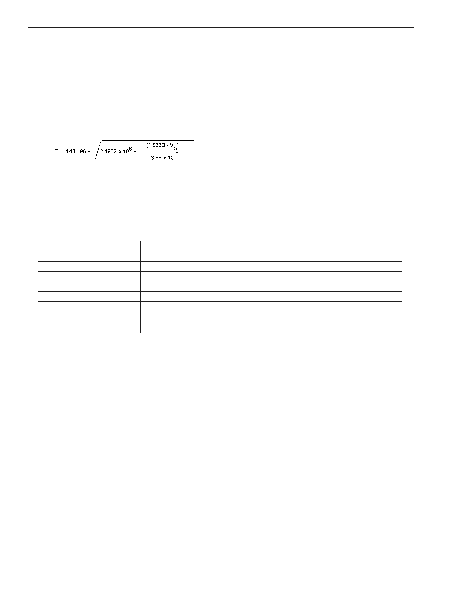
LM20EP Transfer Function
The LM20EP's transfer function can be described in different
ways with varying levels of precision. A simple linear transfer
function, with good accuracy near 25°C, is
V
O
= -11.69 mV/°C x T + 1.8663 V
Over the full operating temperature range of -55°C to
+130°C, best accuracy can be obtained by using the para-
bolic transfer function
V
O
= (-3.88x10
-6
xT
2
) + (-1.15x10
-2
xT) + 1.8639
solving for T:
A linear transfer function can be used over a limited tempera-
ture range by calculating a slope and offset that give best
results over that range. A linear transfer function can be
calculated from the parabolic transfer function of the
LM20EP. The slope of the linear transfer function can be
calculated using the following equation:
m = -7.76 x 10
-6
x T - 0.0115,
where T is the middle of the temperature range of interest
and m is in V/°C. For example for the temperature range of
T
min
=-30 to T
max
=+100°C:
T=35°C
and
m = -11.77 mV/°C
The offset of the linear transfer function can be calculated
using the following equation:
b = (V
OP
(T
max
) + V
OP
(T) + m x (T
max
+T))/2
,
where:
·
V
OP
(T
max
) is the calculated output voltage at T
max
using
the parabolic transfer function for V
O
·
V
OP
(T) is the calculated output voltage at T using the
parabolic transfer function for V
O
.
Using this procedure the best fit linear transfer function for
many popular temperature ranges was calculated in Figure
2. As shown in Figure 2 the error that is introduced by the
linear transfer function increases with wider temperature
ranges.
Mounting
The LM20EP can be applied easily in the same way as other
integrated-circuit temperature sensors. It can be glued or
cemented to a surface. The temperature that the LM20EP is
sensing will be within about +0.02°C of the surface tempera-
ture to which the LM20EP's leads are attached to.
This presumes that the ambient air temperature is almost the
same as the surface temperature; if the air temperature were
much higher or lower than the surface temperature, the
actual temperature measured would be at an intermediate
temperature between the surface temperature and the air
temperature.
To ensure good thermal conductivity the backside of the
LM20EP die is directly attached to the pin 2 GND pin. The
tempertures of the lands and traces to the other leads of the
LM20EP will also affect the temperature that is being
sensed.
Alternatively, the LM20EP can be mounted inside a sealed-
end metal tube, and can then be dipped into a bath or
screwed into a threaded hole in a tank. As with any IC, the
LM20EP and accompanying wiring and circuits must be kept
insulated and dry, to avoid leakage and corrosion. This is
especially true if the circuit may operate at cold temperatures
where condensation can occur. Printed-circuit coatings and
varnishes such as Humiseal and epoxy paints or dips are
often used to ensure that moisture cannot corrode the
LM20EP or its connections.
The thermal resistance junction to ambient (
JA
) is the pa-
rameter used to calculate the rise of a device junction tem-
perature due to its power dissipation. For the LM20EP the
equation used to calculate the rise in the die temperature is
as follows:
T
J
= T
A
+
JA
[(V
+
I
Q
) + (V
+
- V
O
) I
L
]
where I
Q
is the quiescent current and I
L
is the load current on
the output. Since the LM20EP's junction temperature is the
actual temperature being measured care should be taken to
minimize the load current that the LM20EP is required to
drive.
The tables shown in Figure 3 summarize the rise in die
temperature of the LM20EP without any loading, and the
thermal resistance for different conditions.
Temperature Range
Linear Equation
V
O
=
Maximum Deviation of Linear Equation
from Parabolic Equation (°C)
T
min
(°C)
T
max
(°C)
-55
+130
-11.79 mV/°C x T + 1.8528 V
±
1.41
-40
+110
-11.77 mV/°C x T + 1.8577 V
±
0.93
-30
+100
-11.77 mV/°C x T + 1.8605 V
±
0.70
-40
+85
-11.67 mV/°C x T + 1.8583 V
±
0.65
-10
+65
-11.71 mV/°C x T + 1.8641 V
±
0.23
+35
+45
-11.81 mV/°C x T + 1.8701 V
±
0.004
+20
+30
-11.69 mV/°C x T + 1.8663 V
±
0.004
FIGURE 2. First order equations optimized for different temperature ranges.
LM20EP
Enhanced
Plastic
www.national.com
5
Document Outline