 | –≠–ª–µ–∫—Ç—Ä–æ–Ω–Ω—ã–π –∫–æ–º–ø–æ–Ω–µ–Ω—Ç: LM221H | –°–∫–∞—á–∞—Ç—å:  PDF PDF  ZIP ZIP |

TL H 7769
LM221LM321
Precision
Preamplifiers
February 1995
LM221 LM321 Precision Preamplifiers
General Description
The LM221 series are precision preamplifiers designed to
operate with general purpose operational amplifiers to dras-
tically decrease dc errors Drift bias current common mode
and supply rejection are more than a factor of 50 better than
standard op amps alone Further the added dc gain of the
LM221 decreases the closed loop gain error
The LM221 series operates with supply voltages from
g
3V
to
g
20V and has sufficient supply rejection to operate from
unregulated supplies The operating current is programma-
ble from 5 mA to 200 mA so bias current offset current gain
and noise can be optimized for the particular application
while still realizing very low drift Super-gain transistors are
used for the input stage so input error currents are lower
than conventional amplifiers at the same operating current
Further the initial offset voltage is easily nulled to zero
The extremely low drift of the LM221 will improve accuracy
on almost any precision dc circuit For example instrumen-
tation amplifier strain gauge amplifiers and thermocouple
amplifiers now using chopper amplifiers can be made with
the LM221 The full differential input and high common-
mode rejection are another advantage over choppers For
applications where low bias current is more important than
drift the operating current can be reduced to low values
High operating currents can be used for low voltage noise
with low source resistance The programmable operating
current of the LM221 allows tailoring the input characteris-
tics to match those of specialized op amps
The LM221 is specified over a
b
25 C to
a
85 C range and
the LM321 over a 0 C to
a
70 C temperature range
Features
Y
Guaranteed drift of LM321A
0 2 mV C
Y
Guaranteed drift of LM221 series
1 mV C
Y
Offset voltage less than 0 4 mV
Y
Bias current less than 10 nA at 10 mA operating current
Y
CMRR 126 dB minimum
Y
120 dB supply rejection
Y
Easily nulled offset voltage
Typical Applications
Thermocouple Amplifier with Cold Junction Compensation
TL H 7769 ≠ 1
Set for 2 98V at output with LM113
shorted Output should equal ambi-
ent temperature at 10 mV K
Adjust for output reading in C
C1995 National Semiconductor Corporation
RRD-B30M115 Printed in U S A

Absolute Maximum Ratings
Supply Voltage
g
20V
Power Dissipation (Note 1)
500 mW
Differential Input Voltage (Notes 2 and 3)
g
15V
Input Voltage (Note 3)
g
15V
Operating Temperature Range
LM321A
0 C to
a
70 C
Storage Temperature Range
b
65 C to
a
150 C
Lead Temperature (Soldering 10 sec )
300 C
ESD rating to be determined
Electrical Characteristics
(Note 4) LM321A
Parameter
Conditions
LM321A
Units
Min
Typ
Max
Input Offset Voltage
T
A
e
25 C 6 4k
s
R
SET
s
70k
0 2
0 4
mV
Input Offset Current
T
A
e
25 C
R
SET
e
70k
0 3
0 5
nA
R
SET
e
6 4k
5
nA
Input Bias Current
T
A
e
25 C
R
SET
e
70k
5
15
nA
R
SET
e
6 4k
50
150
nA
Input Resistance
T
A
e
25 C
R
SET
e
70k
2
8
MX
R
SET
e
6 4k
0 2
MX
Supply Current
T
A
e
25 C R
SET
e
70k
0 8
2 2
mA
Input Offset Voltage
6 4k
s
R
SET
s
70k
0 5
0 65
mV
Input Bias Current
R
SET
e
70k
15
25
nA
R
SET
e
6 4k
150
250
nA
Input Offset Current
R
SET
e
70k
0 5
1
nA
R
SET
e
6 4k
5
10
nA
Input Offset Current Drift
R
SET
e
70k
3
pA C
Average Temperature
R
S
s
200X 6 4k
s
R
SET
s
70k
Coefficient of Input Offset
Offset Voltage Nulled
Voltage
0 07
0 2
m
V C
Long Term Stability
3
m
V yr
Supply Current
1
3 5
mA
Input Voltage Range
V
S
e
g
15V (Note 5)
R
SET
e
70k
g
13
V
R
SET
e
6 4k
a
7
b
13
V
Common-Mode Rejection
R
SET
e
70k
126
140
dB
Ratio
R
SET
e
6 4k
120
130
dB
Supply Voltage Rejection
R
SET
e
70k
118
126
dB
Ratio
R
SET
e
6 4k
114
120
dB
Voltage Gain
T
A
e
25 C R
SET
e
70k
R
L
l
3 MX
12
20
V V
Noise
R
SET
e
70k R
SOURCE
e
0
8
nV
0
Hz
Note 1
The maximum junction temperature of the LM321A is 85 C For operating at elevated temperature devices in the H08 package must be derated based on
a thermal resistance of 150 C W junction to ambient or 18 C W junction to case
Note 2
The inputs are shunted with back-to-back diodes in series with a 500X resistor for overvoltage protection Therefore excessive current will flow if a
differential input voltage in excess of 1V is applied between the inputs
Note 3
For supply voltages less than
g
15V the absolute maximum input voltage is equal to the supply voltage
Note 4
These specifications apply for
g
5
s
V
S
s g
20V and
b
55 C
s
T
A
s a
125 C unless otherwise specified With the LM221A however all temperature
specifications are limited to
b
25 C
s
T
A
s a
85 C and for the LM321A the specifications apply over a 0 C to
a
70 C temperature range
Note 5
External precision resistor
0 1%
can be placed from pins 1 and 8 to 7 increase positive common-mode range
Note 6
See RETS121X for LM121H 883 military specs and RET121AX for LM121AH 883 military specs
2

Absolute Maximum Ratings
If Military Aerospace specified devices are required
please contact the National Semiconductor Sales
Office Distributors for availability and specifications
Supply Voltage
g
20V
Power Dissipation (Note 1)
500 mW
Differential Input Voltage (Notes 2 and 3)
g
15V
Input Voltage (Note 3)
g
15V
Operating Temperature Range
LM221 LM121A (-883) LM121 (-883)
b
25 C to
a
85 C
LM321 LM321A
0 C to
a
70 C
Storage Temperature Range
b
65 C to
a
150 C
Lead Temperature (Soldering 10 sec )
260 C
ESD rating to be determined
Electrical Characteristics
(Note 4) LM221 LM321
Parameter
Conditions
LM221
LM321
Units
Min
Typ
Max
Min
Typ
Max
Input Offset Voltage
T
A
e
25 C 6 4k
s
R
SET
s
70k
0 7
1 5
mV
Input Offset Current
T
A
e
25 C
R
SET
e
70k
1
2
nA
R
SET
e
6 4k
10
20
nA
Input Bias Current
T
A
e
25 C
R
SET
e
70k
10
18
nA
R
SET
e
6 4k
100
180
nA
Input Resistance
T
A
e
25 C
R
SET
e
70k
4
2
MX
R
SET
e
6 4k
0 4
0 2
MX
Supply Current
T
A
e
25 C R
SET
e
70k
1 5
2 2
mA
Input Offset Voltage
6 4k
s
R
SET
s
70k
1 0
2 5
mV
Input Bias Current
R
SET
e
70k
30
28
nA
R
SET
e
6 4k
300
280
nA
Input Offset Current
R
SET
e
70k
3
4
nA
R
SET
e
6 4k
30
40
nA
Input Offset Current Drift
R
SET
e
70k
3
3
pA C
Average Temperature
R
S
s
200X 6 4k
s
R
SET
s
70k
Coefficient of Input
Offset Voltage Nulled
1
1
m
V C
Offset Voltage
Long Term Stability
5
5
m
V yr
Supply Current
2 5
3 5
mA
Input Voltage Range
V
S
e
g
15V (Note 5)
R
SET
e
70k
g
13
g
13
V
R
SET
e
6 4k
a
7
b
13
a
7
b
13
V
Common-Mode Rejection
R
SET
e
70k
120
114
dB
Ratio
R
SET
e
6 4k
114
114
dB
Supply Voltage Rejection
R
SET
e
70k
120
114
dB
Ratio
R
SET
e
6 4k
114
114
dB
Voltage Gain
T
A
e
25 C R
SET
e
70k
R
L
l
3 MX
16
12
V V
Noise
R
SET
e
70k R
SOURCE
e
0
8
8
nV
0
Hz
Note 1
The maximum junction temperature of the LM221 is 100 C The maximum junction temperature of the LM321 is 85 C For operating at elevated
temperature devices in the H08 package must be derated based on a thermal resistance of 150 C W junction to ambient or 18 C W junction to case
Note 2
The inputs are shunted with back-to-back diodes in series with a 500X resistor for overvoltage protection Therefore excessive current will flow if a
differential input voltage in excess of 1V is applied between the inputs
Note 3
For supply voltages less than
g
15V the absolute maximum input voltage is equal to the supply voltage
Note 4
These specifications apply for
g
5
s
V
S
s
g
20V and
b
55 C
s
T
A
s
a
125 C unless otherwise specified With the LM221 however all temperature
specifications are limited to
b
25 C
s
T
A
s a
85 C and for the LM321 the specifications apply over a 0 C to
a
70 C temperature range
Note 5
External precision resistor
0 1%
can be placed from pins 1 and 8 to 7 increase positive common-mode range
3

Typical Performance Characteristics
Input Bias Current
Voltage Drift (Nulled)
Distribution of Offset
Voltage Drift (Nulled)
Distribution of Offset
Rejection
Positive Power Supply
Rejection
Negative Power Supply
Input Noise Voltage
Input Noise Current
Voltage Drift
Differential Voltage Gain
Set Resistor and Set Current
Set Current
Common-Mode Limits
TL H 7769 ≠ 9
4
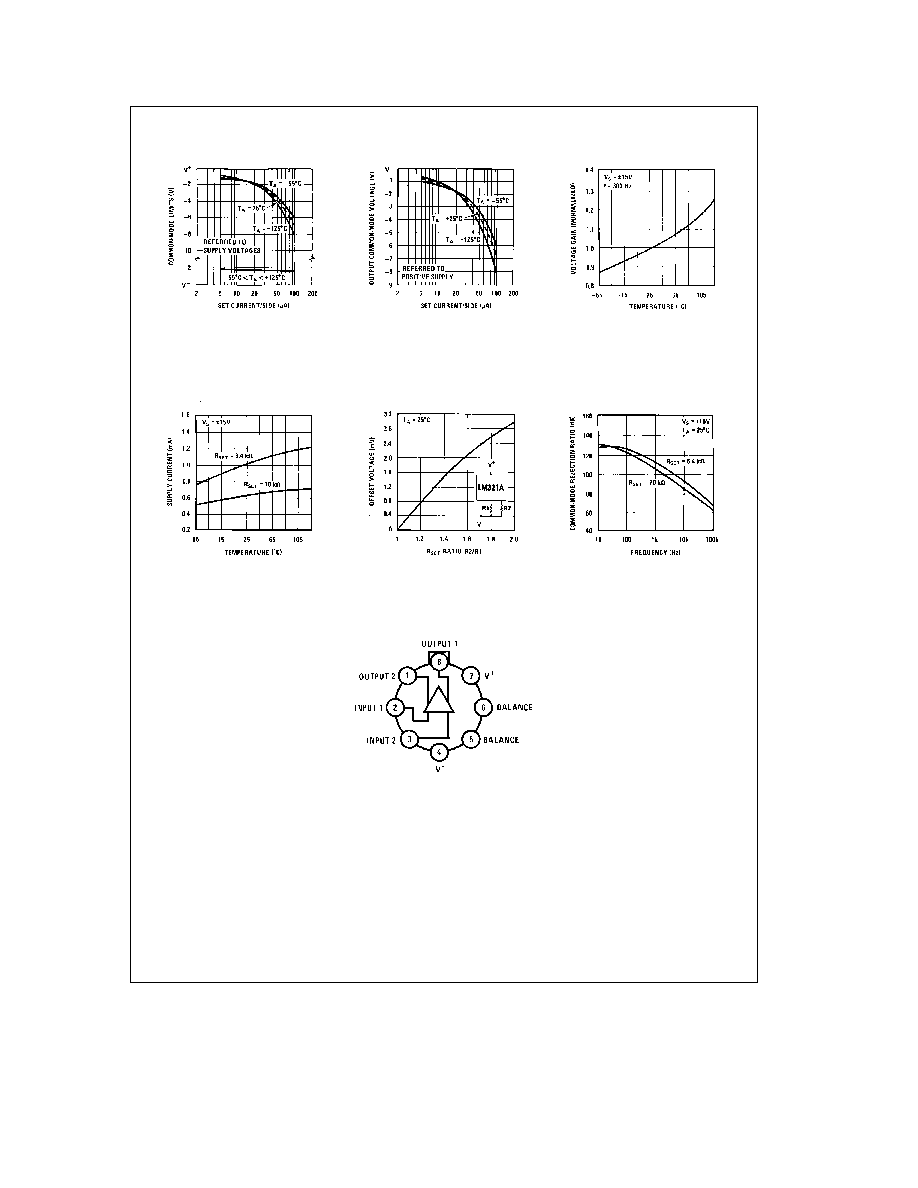
Typical Performance Characteristics
(Continued)
Common-Mode Limits
Output Common-Mode Voltage
Differential Voltage Gain
Supply Current
Offset Voltage Adjustment
Ratio
Common-Mode Rejection
TL H 7769 ≠ 10
Connection Diagram
Metal Can Package
TL H 7769 ≠ 7
Top View
Note
Pin 4 connected to case
Order Number LM121AH 883 LM121H 883
LM221H LM321H or LM321AH
See NS Package Number H08C
Note
Outputs are inverting from the input of the same number
5