LM231A/LM231/LM331A/LM331
Precision Voltage-to-Frequency Converters
General Description
The LM231/LM331 family of voltage-to-frequency converters
are ideally suited for use in simple low-cost circuits for
analog-to-digital conversion, precision frequency-to-voltage
conversion, long-term integration, linear frequency modula-
tion or demodulation, and many other functions. The output
when used as a voltage-to-frequency converter is a pulse
train at a frequency precisely proportional to the applied in-
put voltage. Thus, it provides all the inherent advantages of
the voltage-to-frequency conversion techniques, and is easy
to apply in all standard voltage-to-frequency converter appli-
cations. Further, the LM231A/LM331A attain a new high
level of accuracy versus temperature which could only be at-
tained with expensive voltage-to-frequency modules. Addi-
tionally the LM231/331 are ideally suited for use in digital
systems at low power supply voltages and can provide
low-cost
analog-to-digital
conversion
in
microprocessor-controlled systems. And, the frequency from
a battery powered voltage-to-frequency converter can be
easily channeled through a simple photoisolator to provide
isolation against high common mode levels.
The LM231/LM331 utilize a new temperature-compensated
band-gap reference circuit, to provide excellent accuracy
over the full operating temperature range, at power supplies
as low as 4.0V. The precision timer circuit has low bias cur-
rents without degrading the quick response necessary for
100 kHz voltage-to-frequency conversion. And the output
are capable of driving 3 TTL loads, or a high voltage output
up to 40V, yet is short-circuit-proof against V
CC
.
Features
n
Guaranteed linearity 0.01% max
n
Improved performance in existing voltage-to-frequency
conversion applications
n
Split or single supply operation
n
Operates on single 5V supply
n
Pulse output compatible with all logic forms
n
Excellent temperature stability,
�
50 ppm/�C max
n
Low power dissipation, 15 mW typical at 5V
n
Wide dynamic range, 100 dB min at 10 kHz full scale
frequency
n
Wide range of full scale frequency, 1 Hz to 100 kHz
n
Low cost
Typical Applications
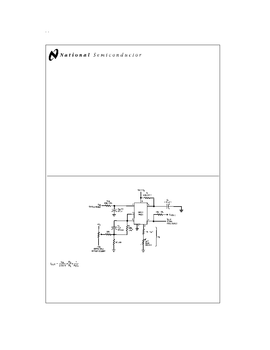
Teflon
�
is a registered trademark of DuPont
DS005680-1
*
Use stable components with low temperature coefficients. See Typical Applications section.
**
0.1�F or 1�F, See "Principles of Operation."
FIGURE 1. Simple Stand-Alone Voltage-to-Frequency Converter
with
�
0.03% Typical Linearity (f = 10 Hz to 11 kHz)
June 1999
LM231A/LM231/LM331A/LM331
Precision
V
oltage-to-Frequency
Converters
� 1999 National Semiconductor Corporation
DS005680
www.national.com
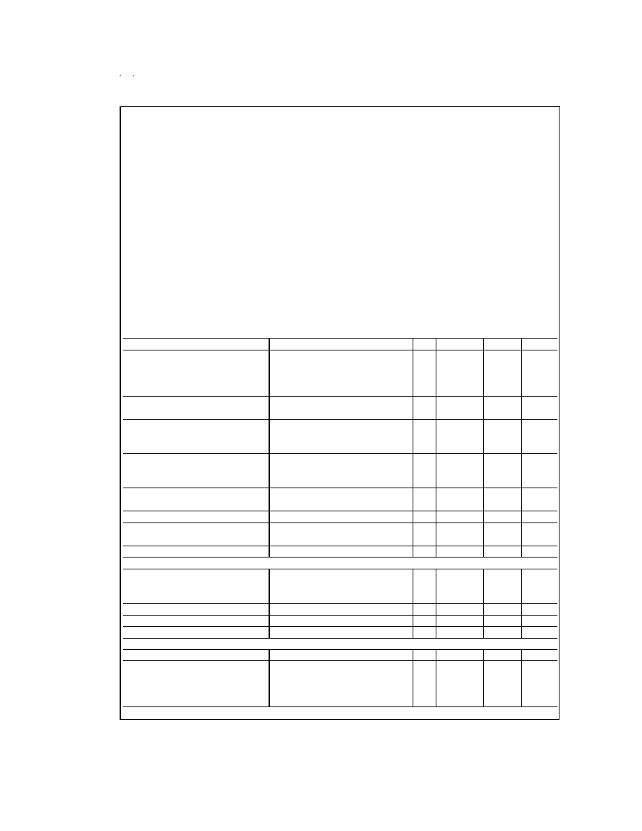
Absolute Maximum Ratings
(Note 1)
If Military/Aerospace specified devices are required, please contact the National Semiconductor Sales Office/
Distributors for availability and specifications.
LM231A/LM231
LM331A/LM331
Supply Voltage
40V
40V
Output Short Circuit to Ground
Continuous
Continuous
Output Short Circuit to V
CC
Continuous
Continuous
Input Voltage
-0.2V to +V
S
-0.2V to +V
S
T
MIN
T
MAX
T
MIN
T
MAX
Operating Ambient Temperature Range
-25�C to +85�C
0�C to +70�C
Power Dissipation (P
D
at 25�C)
and Thermal Resistance (
jA
)
(N Package) P
D
1.25W
1.25W
jA
100�C/W
100�C/W
Lead Temperature (Soldering, 10 sec.)
Dual-In-Line Package (Plastic)
260�C
260�C
ESD Susceptibility (Note 4)
N Package
500V
500V
Electrical Characteristics
T
A
=25�C unless otherwise specified (Note 2)
Parameter
Conditions
Min
Typ
Max
Units
VFC Non-Linearity (Note 3)
4.5V
V
S
20V
�
0.003
�
0.01
% Full-
Scale
T
MIN
T
A
T
MAX
�
0.006
�
0.02
% Full-
Scale
VFC Non-Linearity
V
S
= 15V, f = 10 Hz to 11 kHz
�
0.024
�
0.14
%Full-
In Circuit of
Figure 1
Scale
Conversion Accuracy Scale Factor (Gain)
V
IN
= -10V, R
S
= 14 k
LM231, LM231A
0.95
1.00
1.05
kHz/V
LM331, LM331A
0.90
1.00
1.10
kHz/V
Temperature Stability of Gain
T
MIN
T
A
T
MAX
, 4.5V
V
S
20V
LM231/LM331
�
30
�
150
ppm/�C
LM231A/LM331A
�
20
�
50
ppm/�C
Change of Gain with V
S
4.5V
V
S
10V
0.01
0.1
%/V
10V
V
S
40V
0.006
0.06
%/V
Rated Full-Scale Frequency
V
IN
= -10V
10.0
kHz
Gain Stability vs Time
T
MIN
T
A
T
MAX
�
0.02
% Full-
(1000 Hrs)
Scale
Overrange (Beyond Full-Scale) Frequency
V
IN
= -11V
10
%
INPUT COMPARATOR
Offset Voltage
�
3
�
10
mV
LM231/LM331
T
MIN
T
A
T
MAX
�
4
�
14
mV
LM231A/LM331A
T
MIN
T
A
T
MAX
�
3
�
10
mV
Bias Current
-80
-300
nA
Offset Current
�
8
�
100
nA
Common-Mode Range
T
MIN
T
A
T
MAX
-0.2
V
CC
-2.0
V
TIMER
Timer Threshold Voltage, Pin 5
0.63
0.667
0.70
x V
S
Input Bias Current, Pin 5
V
S
= 15V
All Devices
0V
V
PIN 5
9.9V
�
10
�
100
nA
LM231/LM331
V
PIN 5
= 10V
200
1000
nA
LM231A/LM331A
V
PIN 5
= 10V
200
500
nA
www.national.com
2
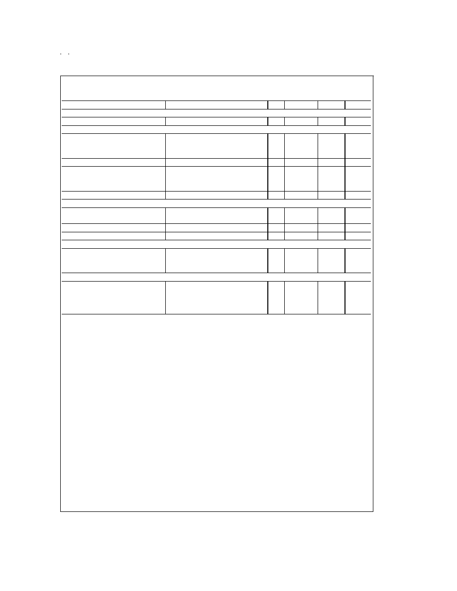
Electrical Characteristics
(Continued)
T
A
=25�C unless otherwise specified (Note 2)
Parameter
Conditions
Min
Typ
Max
Units
TIMER
V
SAT PIN 5
(Reset)
I = 5 mA
0.22
0.5
V
CURRENT SOURCE (Pin 1)
Output Current
R
S
=14 k
, V
PIN 1
=0
LM231, LM231A
126
135
144
�A
LM331, LM331A
116
136
156
�A
Change with Voltage
0V
V
PIN 1
10V
0.2
1.0
�A
Current Source OFF Leakage
LM231, LM231A, LM331, LM331A
0.02
10.0
nA
All Devices
T
A
=T
MAX
2.0
50.0
nA
Operating Range of Current (Typical)
(10 to 500)
�A
REFERENCE VOLTAGE (Pin 2)
LM231, LM231A
1.76
1.89
2.02
V
DC
LM331, LM331A
1.70
1.89
2.08
V
DC
Stability vs Temperature
�
60
ppm/�C
Stability vs Time, 1000 Hours
�
0.1
%
LOGIC OUTPUT (Pin 3)
V
SAT
I=5 mA
0.15
0.50
V
I=3.2 mA (2 TTL Loads), T
MIN
T
A
T
MAX
0.10
0.40
V
OFF Leakage
�
0.05
1.0
�A
SUPPLY CURRENT
LM231, LM231A
V
S
=5V
2.0
3.0
4.0
mA
LM331, LM331A
V
S
=40V
2.5
4.0
6.0
mA
V
S
=5V
1.5
3.0
6.0
mA
V
S
=40V
2.0
4.0
8.0
mA
Note 1: Absolute Maximum Ratings indicate limits beyond which damage to the device may occur. DC and AC electrical specifications do not apply when operating
the device beyond its specified operating conditions.
Note 2: All specifications apply in the circuit of
Figure 4, with 4.0V
V
S
40V, unless otherwise noted.
Note 3: Nonlinearity is defined as the deviation of f
OUT
from V
IN
x (10 kHz/-10 V
DC
) when the circuit has been trimmed for zero error at 10 Hz and at 10 kHz, over
the frequency range 1 Hz to 11 kHz. For the timing capacitor, C
T
, use NPO ceramic, Teflon
�
, or polystyrene.
Note 4: Human body model, 100 pF discharged through a 1.5 k
resistor.
www.national.com
3

Functional Block Diagram
DS005680-2
Pin numbers apply to 8-pin packages only.
FIGURE 2.
www.national.com
4

Typical Performance Characteristics
(All electrical characteristics apply for the circuit of
Figure 4, unless otherwise noted.)
Nonlinearity Error
as Precision V-to-F
Converter (
Figure 4)
DS005680-25
Nonlinearity Error
DS005680-26
Nonlinearity Error vs Power
Supply Voltage
DS005680-27
Frequency vs Temperature
DS005680-28
V
REF
vs Temperature
DS005680-29
Output Frequency vs
V
SUPPLY
DS005680-30
100 kHz Nonlinearity Error
(
Figure 5)
DS005680-31
Nonlinearity Error
(
Figure 1)
DS005680-32
Input Current (Pins 6,7) vs
Temperature
DS005680-33
www.national.com
5