 | ÐлекÑÑоннÑй компоненÑ: LM2408 | СкаÑаÑÑ:  PDF PDF  ZIP ZIP |
Äîêóìåíòàöèÿ è îïèñàíèÿ www.docs.chipfind.ru
TL H 12683
LM2408
Monolithic
Triple
45
ns
CRT
Driver
December 1996
LM2408
Monolithic Triple 4 5 ns CRT Driver
General Description
The LM2408 is an integrated high voltage CRT driver circuit
designed for use in color monitor applications The IC con-
tains three high input impedance wide band amplifiers
which directly drive the RGB cathodes of a CRT The gain of
each channel is internally set at
b
15 and can drive CRT
capacitive loads as well as resistive loads presented by oth-
er applications limited only by the package's power dissipa-
tion
The IC is packaged in an industry standard 11-Lead TO-220
molded plastic power package See thermal considerations
on page 5
Features
Y
Rise fall times typically 4 5 ns with 8 pF load
Y
Output swing capability 50 V
PP
for V
CC
e
80
40 V
PP
for V
CC
e
70
30 V
PP
for V
CC
e
60
Y
Pinout designed for easy PCB layout
Y
1V to 7V input range
Y
Stable with 0 pF 20 pF capactive loads
Y
Convenient TO-220 staggered lead package style
Applications
Y
CRT driver for 1280
c
1024 (Non-interfaced) and XGA
display resolution color monitors
Y
Pixel clock frequency up to 160 MHz
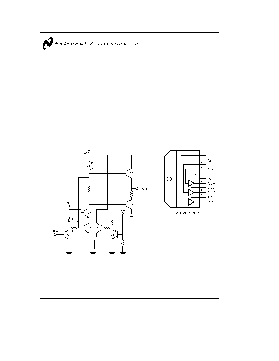
Schematic and Connection Diagrams
TL H 12683 1
FIGURE 1 Simplified Schematic Diagram (One Channel)
TL H 12683 2
Note
Tab is at GND
Top View
C1996 National Semiconductor Corporation
RRD-B30M126 Printed in U S A
http
www national com
Absolute Maximum Ratings
(Notes 1 and 3)
Supply Voltage (V
CC
)
a
95V
Bias Voltage (V
BB
)
a
16V
Input Voltage (V
IN
)
b
0 5V to V
BIAS
a
0 5V
Storage Temperature Range (T
STG
)
b
65 C to
a
150 C
Lead Temperature (Soldering
k
10 sec )
300 C
ESD Tolerance
2 kV
Operating Ranges
(Note 2)
V
CC
a
60V to
a
85V
V
BB
a
8V to
a
15V
V
IN
a
1V to
a
7V
Case Temperature (T
CASE
)
b
20 C to
a
100 C
Do not operate the part without a heat sink
Electrical Characteristics
Unless otherwise noted V
CC
e a
80V V
BB
e a
12V V
IN
e a
3 2V (at LM2408 input pins) C
L
e
8 pF Output
e
40 V
PP
at
1 MHz T
A
e
25 C
Symbol
Parameter
Conditions
LM2408
Units
Min
Typical
Max
I
CC
Supply Current
Per Channel No Output Load
22
30
mA
I
BB
Bias Current
21
mA
V
OUT
DC Output Voltage
No Input Signal
47
50
53
V
DC
A
V
DC Voltage Gain
No Input Signal
b
13
b
15
b
17
D
A
V
Gain Matching
(Note 4)
1 0
dB
LE
Linearity Error
(Notes 4 5)
8
%
t
R
Rise Time
10% to 90% f
e
1 MHz
4 5
ns
t
F
Fall Time
90% to 10% f
e
1 MHz
4 5
ns
Note 1
Absolute Maximum Ratings indicate limits beyond which damage to the device may occur
Note 2
Operating ratings indicate conditions for which the device is functional but do not guarantee specific performance limits For guaranteed specifications and
test conditions see the Electrical Characteristics The guaranteed specifications apply only for the test conditions listed Some performance characteristics may
change when the device is not operated under the listed test conditions
Note 3
All voltages are measured with respect to GND unless otherwise specified
Note 4
Calculated value from Voltage Gain test on each channel
Note 5
Linearity Error is defined as the variation in DC gain from V
IN
e a
1 90V to V
IN
e a
4 50V
Note 6
Input from signal generator t
R
t
F
k
1 ns
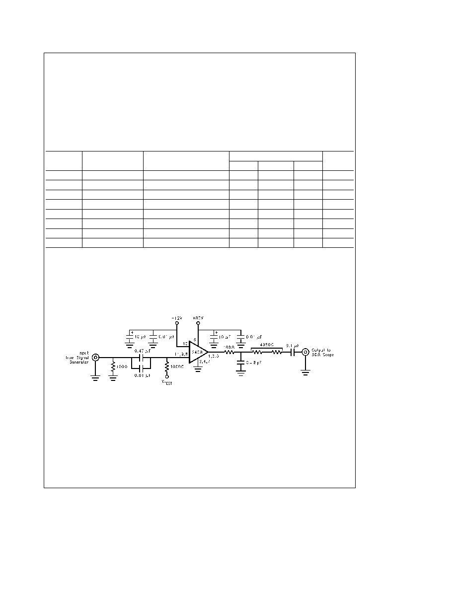
AC Test Circuit
TL H 12683 3
Note
8 pF is total load plus parasitic capacitance
Note
Adjust Vtest for
a
3 2V DC at LM2408 input pins
FIGURE 2 Test Circuit (One Channel)
Figure 2 shows a typical test circuit for evaluation of the
LM2408 This circuit is designed to allow testing of the
LM2408 in a 50X environment such as a pulse generator
oscilloscope or network analyzer The 4950X resistor at the
output forms a 100 1 voltage divider when connected to a
50X load
http
www national com
2
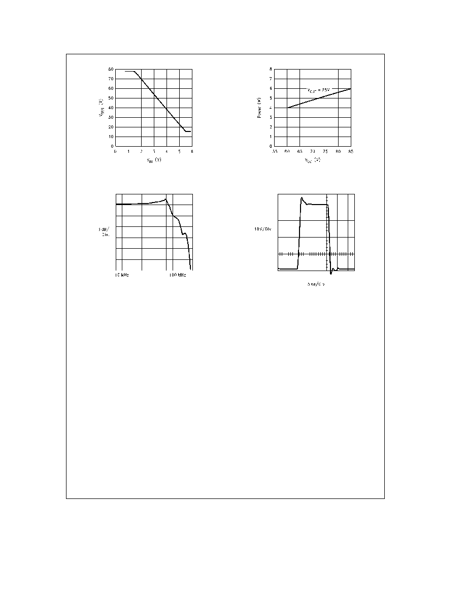
TL H 12683 4
FIGURE 3 V
OUT
vs V
IN
TL H 12683 5
FIGURE 4 Power Dissipation vs V
CC
TL H 12683 6
FIGURE 5 Large Signal Frequency Response
TL H 12683 7
FIGURE 6 Pulse Response
http
www national com
3
Theory of Operation
The LM2408 is a high voltage monolithic triple CRT driver
suitable for SVGA and XGA display applications
The
LM2408 features
a
80V operation and low power dissipa-
tion The part is housed in the industry standard 11-Lead
TO-220 molded plastic power package
The simplified circuit diagram of the LM2408 is shown in
Figure 1 A PNP emitter follower Q1 provides input buffer-
ing Q2 and Q3 form a high gain amplifier Feedback around
this amplifier through the 15 kX resistor working with the
1 kX input resistor sets the gain to
b
15 Emitter followers
Q5 and Q6 isolate the high output impedance of the amplifi-
er from the capacitance of the CRT cathode and make the
circuit relative insensitive to load capacitance
Figure 2 shows a typical test circuit for evaluation of the
LM2408 This circuit is designed to allow testing of the
LM2408 in a 50X environment such as a pulse generator
and a scope or a network analyzer In this test circuit two
low inductance resistors in series totaling 4 95 kX form a
100 1 wideband low capacitance probe when connected to
a 50X cable and load The input signal from the generator is
AC coupled to the base of Q1
Application Hints
INTRODUCTION
National Semiconductor is committed to providing applica-
tion information that assists our customers in obtaining the
best performance possible from our products The following
information is provided in order to support this commitment
The reader should be aware that the optimization of per-
formance was done using specific printed circuit boards de-
signed at National Variations in performance can be real-
ized due to physical changes in the printed circuit board and
the application Therefore the designer should be aware
that component value and board layout changes may be
required to optimize performance in a given application The
values shown in this document can be used as a staring
point for testing and evaluation purposes When working
with high bandwidth circuits good layout practices are also
critical to achieving maximum performance
POWER SUPPLY BYPASS
Since the LM2408 is a wide bandwidth amplifier proper
power supply bypassing is critical for optimum performance
Improper power supply bypassing can result in large over-
shoot ringing and oscillation A 0 01 mF capacitor should be
connected from the supply pin V
CC
to ground as close to
the supply pin as is practical (preferably less than
from
the supply pin) Additionally a 10 mF to 100 mF electrolytic
capacitor should be connected from the supply pin to
ground The electrolytic capacitor should also be placed
reasonably close to the LM2408's supply pin A 0 1 mF ca-
pacitor should be connected from the bias pin V
BB
to
ground as close as is practical to the part
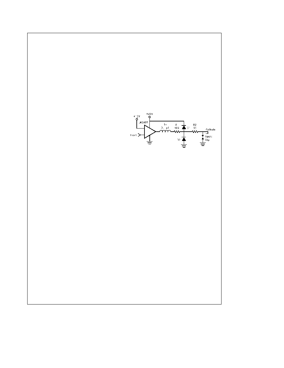
ARC PROTECTION
During normal CRT operation internal arcing may occasion-
ally occur Spark gaps of 200V to 300V at the cathodes will
limit the maximum voltage but to a value that is much high-
er than allowable on the LM2408 This fast high voltage
high energy pulse can damage the LM2408 output stage
The addition of clamp diodes D1 and D2 (as shown in
Fig-
ure 7 ) will help clamp the voltage at the output of the
LM2408 to a safe level The clamp diodes should have a
fast transient response high peak current rating low series
impedance and low shunt capacitance FDH400 or equiva-
lent diodes are recommended Resistor R2 in
Figure 7 limits
the arcover current while R1 limits the current into the
LM2408 and reduces the power dissipation of the output
transistors when the output is stressed beyond the supply
voltage Peaking inductor Lp also helps protect the LM2408
from CRT arcover and is part of the arc protection circuit
Having large value resistors for R1 and R2 would be desir-
able but this has the effect of increasing rise and fall times
For proper arc protection it is important to not omit any of
the arc protection components shown in
Figure 7
TL H 12683 8
FIGURE 7 One Section of the LM2408 with Arc
Protection and Peaking Inductor L
P
There are also ESD protection diodes built into the part To
avoid damaging these diodes do not apply an input voltage
from a low impedance source when the V
BB
and V
CC
pins
are held at ground potential
IMPROVING RISE AND FALL TIMES
Because of an emitter follower output stage the rise and fall
times of the LM2408 are relatively insensitive to capactive
loading However the series resistors R1 and R2 (see
Fig-
ure 7 ) will increase the rise and fall times when driving the
CRT's cathode which appears as a capacitive load The ca-
pacitance at the cathode typically ranges from 8 pF to
12 pF
To improve the rise and fall times at the cathode a small
inductor is often used in series with the output of the amplifi-
er The inductor L
P
in
Figure 7 peaks the amplifier's frequen-
cy response at the cathode thus improving rise and fall
times It also acts with the output load capacitance to form a
low pass filter which reduces the amplitudes of high fre-
quency harmonics of the video signal to lower radiated
electromagnetic interference The inductor value is empiri-
cally determined and is dependent on the load An inductor
value of 0 1 mH is a good starting value Note that excessive
peaking of the amplifier's frequency response will increase
the overshoot Choosing the correct values for R1 R2 and
Lp will provide arc protection and the fastest rise and fall
times without excessive peaking
http
www national com
4
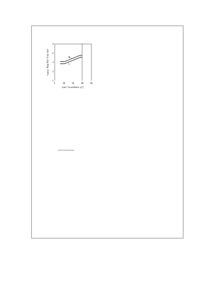
EFFECT OF LOAD CAPACITANCE
The output rise and fall times will be slower than specified if
the load capacitance at the output is more than 8 pF as
shown in
Figure 8
TL H 12683 9
FIGURE 8 Effect of Load Capacitance on
Rise Fall Time
The monitor designer should ensure that stray capacitance
applied to the LM2408 is as low as possible
THERMAL CONSIDERATIONS
Power supply current increases as the input signal increas-
es and consequently power dissipation also increases
The LM2408 cannot be used without heat sinking Typical
``average'' power dissipation with the device output voltage
at one half the supply voltage is 1 9W per channel for a total
dissipation of 5 7W package dissipation The power dissipa-
tion does not vary much as output voltage varies The
LM2408 case temperature must be maintained below
100 C If the maximum expected ambient temperature is
50 C then a maximum heat sink thermal resistance can be
calculated
R
th
e
100 C
b
50 C
5 7W
e
8 8 C W
This example assumes a typical CRT capacitive load and is
without a resistive load Note that this thermal resistance
must be achieved when the heat sink is operating in the
monitor
PC BOARD LAYOUT CONSIDERATIONS
For optimum performance an adequate ground plane isola-
tion between channels good supply bypassing and minimiz-
ing unwanted feedback are necessary Also the length of
the signal traces from the preamplifier to the LM2408 and
from the LM2408 to the CRT cathode should be as short as
possible The following references are recommended
Ott Henry W ``Noise Reduction Techniques in Electronic
Systems'' John Wiley and Sons New York 1976
``Guide to CRT Video Design'' National Semiconductor Ap-
plication Note 861
``Video Amplifier Design for Computer Monitors'' National
Semiconductor Application Note 1013
Because of its high small signal bandwidth the part may
oscillate when it is used in a typical application with a
preamp in a monitor if feedback occurs around the video
amplifier through the chassis wiring To prevent this leads
to the input circuit should be shielded and input circuit wir-
ing should be spaced as far as possible from output circuit
wiring Power should be removed as quickly as possible
from an amplifier that is oscillating since power dissipation
in the part is very high in this mode and the part may be
damaged if oscillations continue and the power supply can
supply more than 250 mA
Capacitive loading on the output will cause some overshoot
and peaking This can be controlled by placing a resistor in
series with the output of the part Because of differences in
stray capacitance in different pc board layouts the best val-
ue of resistance to use must be determined separately for
each application Typical values between 50X and 200X
provide good performance with the larger values resulting
in less peaking and slower rise and fall times
Driving the output voltage of the part outside of its linear
range will cause distorted signal waveforms and recovery
times that are very much longer than the specified rise and
fall times When the amplifier output voltage is being driven
from positive saturation into the linear range an overshoot
of several volts for up to 50 ns may occur In a typical moni-
tor design this may occur if blanking pulses are applied to
the video signal The output voltage range should be limited
so this does not happen and will be approximately no lower
than 25V and no higher than V
CC
b
5V
TYPICAL APPLICATION
A typical application of the LM2408 is shown in
Figure 9
Used in conjunction with an LM1205 a complete video
channel from monitor input to CRT cathode can be
achieved Performance is satisfactory for all applications up
to 1280
c
1024 non-interfaced and pixel clock frequencies
up to 160 MHz
http
www national com
5