 | –≠–ª–µ–∫—Ç—Ä–æ–Ω–Ω—ã–π –∫–æ–º–ø–æ–Ω–µ–Ω—Ç: LM2413 | –°–∫–∞—á–∞—Ç—å:  PDF PDF  ZIP ZIP |

LM2413
Monolithic Triple 4 ns CRT Driver
General Description
The LM2413 is an integrated high voltage CRT driver circuit
designed for use in high-resolution color monitor applica-
tions. The IC contains three high input impedance, wide
band amplifiers, which directly drive the RGB cathodes of a
CRT. Each channel has its gain internally set to -14 and can
drive CRT capacitive loads as well as resistive loads present
in other applications, limited only by the package's power
dissipation.
The IC is packaged in an industry standard 11 lead TO-220
molded plastic power package. See Thermal Considerations
on page 6.
Features
n
Rise/Fall times typically 3.7/4.4 with 8 pF load at 40 V
PP
n
Well matched with LM1282/3 video preamps
n
1V to 5V input range
n
Stable with 0≠20 pF capacitive loads and inductive
peaking networks
n
Convenient TO-220 staggered lead package style
n
Standard LM240X Family Pinout which is designed for
easy PCB layout
Applications
n
1600 x 1200 Displays up to 70 Hz Refresh
n
Pixel clock frequencies up to 180 MHz
n
Monitors using video blanking
Schematic and Connection Diagrams
DS101275-1
FIGURE 1. Simplified Schematic Diagram (One
Channel)
DS101275-2
Top View
Order Number LM2413T
See NS Package Number TA11C
December 1999
LM2413
Monolithic
T
riple
4
n
s
CRT
Driver
© 1999 National Semiconductor Corporation
DS101275
www.national.com
Absolute Maximum Ratings
(Notes 1, 3)
If Military/Aerospace specified devices are required,
please contact the National Semiconductor Sales Office/
Distributors for availability and specifications.
Supply Voltage, V
CC
+90V
Bias Voltage, V
BB
+16V
Input Voltage, V
IN
0V to 6V
Storage Temperature Range,T
STG
-65∞C to +150∞C
Lead Temperature (Soldering,
10 sec.)
300∞C
ESD Tolerance, Human Body Model
2kV
Machine Model
250V
Operating Ranges
(Note 2)
V
CC
+60V to +85V
V
BB
+10V to +15V
V
IN
+1V to +5V
V
OUT
+15 to +75V
Case Temperature
-20∞C to +100∞C
Do not operate the part without a heat sink.
Electrical Characteristics
(See
Figure 2 for Test Circuit)
Unless otherwise noted: V
CC
= +80V, V
BB
= +12V, V
IN
= +3.3V, No AC Input, C
L
= 8pF, T
C
= 60∞C
Symbol
Parameter
Conditions
LM2413
Units
Min
Typ
Max
I
CC
Supply Current
Per Channel, No Output Load
10
16
22
mA
I
BB
Bias Current
All three channels
15
25
35
mA
V
OUT
DC Output Voltage
V
IN
= 1.9V
62
65
68
V
DC
A
V
DC Voltage Gain
-12
-14
-16
A
V
Gain Matching
(Note 4)
1.0
dB
LE
Linearity Error
(Notes 4, 5)
3.5
%
t
R
Rise Time (Notes 6, 7)
10% to 90%, 40 V
PP
Output (1 MHz)
3.7
4.7
ns
t
F
Fall Time (Notes 6, 7)
90% to 10%, 40 V
PP
Output (1 MHz)
4.4
5.4
ns
OS
Overshoot (Note 6)
(Note 6), 40 V
PP
Output (1 MHz)
5
%
Note 1: Absolute Maximum Ratings indicate limits beyond which damage to the device may occur.
Note 2: Operating ratings indicate conditions for which the device is functional, but do not guarantee specific performance limits. For guaranteed specifications and
test conditions, see the Electrical Characteristics. The guaranteed specifications apply only for the test conditions listed. Some performance characteristics may
change when the device is not operated under the listed test conditions.
Note 3: All voltages are measured with respect to GND, unless otherwise specified.
Note 4: Calculated value from Voltage Gain test on each channel.
Note 5: Linearity Error is the variation in dc gain from V
IN
= 1.6V to V
IN
= 5V.
Note 6: Input from signal generator: t
r
, t
f
<
1 ns.
Note 7: 100% tested in production. These limits are not used to calculate outgoing quality levels.
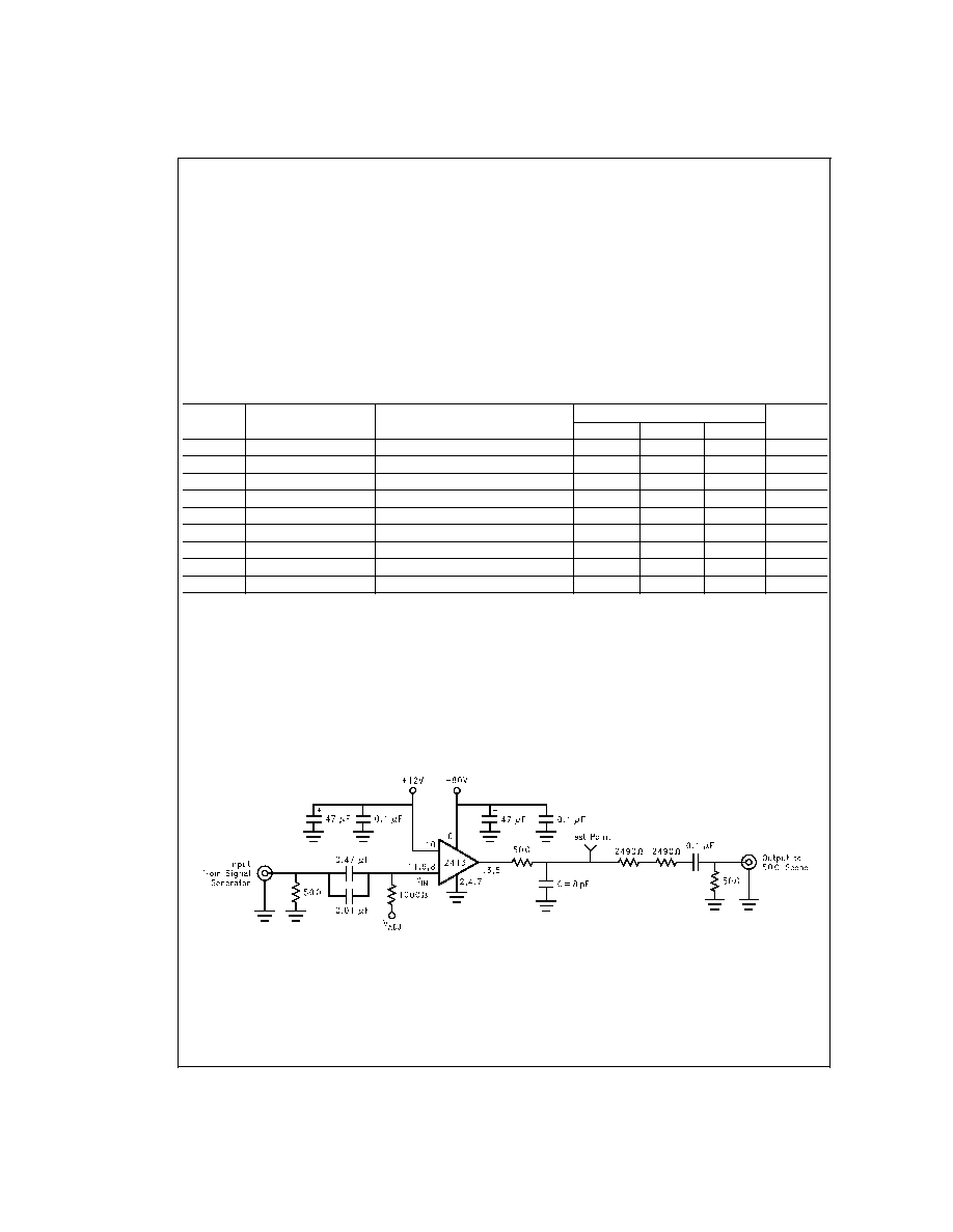
AC Test Circuit
Figure 2 shows a typical test circuit for evaluation of the
LM2413. This circuit is designed to allow testing of the
LM2413 in a 50
environment without the use of an expen-
sive FET probe. The combined resistors of 4950
at the out-
put form a 200:1 voltage divider when connected to a 50
load. The compensation cap is used to flatten the frequency
response of the 200:1 divider.
DS101275-3
FIGURE 2. Test Circuit (One Channel)
LM2413
www.national.com
2

AC Test Circuit
(Continued)
DS101275-4
FIGURE 3. V
IN
vs V
OUT
DS101275-5
FIGURE 4. Speed vs Temp
DS101275-6
FIGURE 5. Rise/Fall Time
DS101275-7
FIGURE 6. Power Dissipation vs Frequency
DS101275-8
FIGURE 7. Speed vs Offset
DS101275-9
FIGURE 8. Bandwidth
LM2413
www.national.com
3

Theory of Operation
The LM2413 is a high voltage monolithic three channel CRT
driver suitable for very high resolution display applications,
up to 1600 x 1200 at 70 Hz refresh rate. The LM2413 oper-
ates using 80V and 12V power supplies. The part is housed
in the industry standard 11-lead TO-220 molded plastic
power package.
The simplified circuit diagram of one channel of the LM2413
is shown in
Figure 1. A PNP emitter follower, Q5, provides in-
put buffering. This minimizes the current loading of the video
pre-amp. R9 is used to turn on Q5 when there is no input.
With Q5 turn on, Q1 will be almost completely off, minimizing
the current flow through Q1 and Q2. This will drive the output
stage near the V
CC
rail, minimizing the power dissipation
with no inputs. R6 is a pull-up resistor for Q5 and also limits
the current flow through Q5. R3 and R2 are used to set the
current flow through Q1 and Q2. The ratio of R1 to R2 is
used to set the gain of the LM2413. R1, R2, and R3 are all
related when calculating the output voltage of the CRT
driver. R
b
limits the current through the base of Q2. Q1 and
Q2 are in a cascode configuration. Q1 is a low voltage and
very fast transistor. Q2 is a higher voltage transistor. The
cascode configuration gives the equivalent of a very fast and
high voltage transistor. The two output transistors, Q3 and
Q4, form a class B amplifier output stage. R4 and R5 are
used to limit the current through the output stage and set the
output impedance of the LM2413. Q6, along with R7 and R8
set the bias current through Q3 and Q4 when there is no
change in the signal level. This bias current minimizes the
crossover distortion of the output stage. With this bias cur-
rent the output stage now becomes a class AB amplifier with
a crossover distortion much lower than a class B amplifier.
Figure 2 shows a typical test circuit for evaluation of the
LM2413. Due to the very wide bandwidth of the LM2413, a
specially designed output circuit is used with the required se-
ries resistor and C
LOAD
to emulate the actual application
when evaluating the performance of the LM2413 in a 50
environment without the use of an expensive FET probe.
The combined resistors of 4950
at the output form a 200:1
voltage divider when connected to a 50
load. The input sig-
nal from the generator is ac coupled to the input of the CRT
driver. V
ADJ
input sets the DC operating range of the
LM2413.
Application Hints
INTRODUCTION
National Semiconductor (NSC) is committed to providing ap-
plication information that assists our customers in obtaining
the best performance possible from our products. The follow-
ing information is provided in order to support this commit-
ment. The reader should be aware that the optimization of
performance was done using a specific printed circuit board
designed at NSC. Variations in performance can be realized
due to physical changes in the printed circuit board and the
application. Therefore, the designer should know that com-
ponent value changes may be required in order to optimize
performance in a given application. The values shown in this
document can be used as a starting point for evaluation pur-
poses. When working with high bandwidth circuits, good lay-
out practices are also critical to achieving maximum perfor-
mance.
POWER SUPPY BYPASS
Since the LM2413 is a very high bandwidth amplifier, proper
power supply bypassing is critical for optimum performance.
Improper power supply bypassing can result in large over-
shoot, ringing and oscillation. A 0.1 µF capacitor should be
connected from the supply pin, V
CC
, to ground, as close to
the supply and ground pins as is practical. Additionally, a 10
µF to 100 µF electrolytic capacitor should be connected from
the supply pin to ground. The electrolytic capacitor should
also be placed reasonably close to the LM2413's supply and
ground pins. A 0.1 µF capacitor should be connected from
the bias pin, V
BB
, to ground, as close as is practical to the
part.
ARC PROTECTION
During normal CRT operation, internal arcing may occasion-
ally occur. Spark gaps, in the range of 200V, connected from
the CRT cathodes to CRT ground will limit the maximum volt-
age, but to a value that is much higher than allowable on the
LM2413. This fast, high voltage, high-energy pulse can dam-
age the LM2413 output stage. The application circuit shown
in
Figure 9 is designed to help clamp the voltage at the out-
put of the LM2413 to a safe level. The clamp diodes should
have a fast transient response, high peak current rating, low
series impedance and low shunt capacitance. FDH400 or
equivalent diodes are recommended. D1 and D2 should
have short, low impedance connections to V
CC
and ground
respectively. The cathode of D1 should be located very close
to a separately decoupled bypass capacitor. The ground
connection of the diode and the decoupling capacitor should
be very close to the LM2413 ground. This will significantly re-
duce the high frequency voltage transients that the LM2413
would be subjected to during an arc-over condition. Resistor
R2 limits the arc-over current that is seen by the diodes while
R1 limits the current into the LM2413 as well as the voltage
stress at the outputs of the device. R2 should be a 1/2W
solid carbon type resistor. R1 can be a 1/4W metal or carbon
film type resistor. Inductor L1 is critical to reduce the inital
high frequency voltage levels that the LM2413 would be sub-
jected to during an arc-over. Having large value resistors for
R1 and R2 would be desirable, but this has the effect of in-
creasing rise and fall times. The inductor will not only help
protect the device but it will also help optimize rise and fall
times as well as minimize EMI. For proper arc protection, it is
important to not omit any of the arc protection components
shown in
Figure 9. The values of L1 and R1 may need to be
adjusted for a particular application. The recommended mini-
mum value for R1 is 110
, with L1 = .12 µH.
LM2413
www.national.com
4

Application Hints
(Continued)
OPTIMIZING TRANSIENT RESPONSE
Referring to
Figure 9, there are three components (R1, R2
and L1) that can be adjusted to optimize the transient re-
sponse of the application circuit. Increasing the values of R1
and R2 will slow the circuit down while decreasing over-
shoot. Increasing the value of L1 will speed up the circuit as
well as increase overshoot. It is very important to use induc-
tors with very high self-resonant frequencies, preferably
above 300 MHz. The values shown in
Figure 9 can be used
as a good starting point for the evaluation of the LM2413.
Effect of Load Capacitance
The output rise and fall times as well as overshoot will vary
as the load capacitance varies. The values of the output cir-
cuit (R1, R2 and L1 in
Figure 9) should be chosen based on
the nominal load capacitance. Once this is done the perfor-
mance of the design can be checked by varying the load
based on what the expected variation will be during produc-
tion.
Effect of Offset
Figure 5 shows the variation in rise and fall times when the
output offset of the device is varied from 35 to 55 VDC. The
rise and fall times show about the same overall variation.
The slightly faster rise and fall times are fastest near the cen-
ter point of 45V, making this the optimum operating point. At
the low and high output offset range, the characteristic of
rise/fall time is slower due to the saturation of Q3 and Q4.
The recovery time of the output transistors takes longer com-
ing out of saturation thus slows down the rise and fall times.
THERMAL CONSIDERATIONS
Figure 4 shows the performance of the LM2413 in the test
circuit shown in
Figure 2 as a function of case temperature.
Figure 4 shows that both the rise and fall times of the
LM2413 become slightly longer as the case temperature in-
creases from 40∞C to 100∞C. Please note that the LM2413 is
never to be operated over a case temperature of 100∞C.
In addition to exceeding the safe operating temperature, the
rise and fall times will typically exceed 3.7/4.4 ns.
Figure 6 shows that total power dissipation of the LM2413
vs. Frequency when all three channels of the device are driv-
ing an 8 pF load. Typically the active time is about 72% of the
total time for one frame. Worst-case power dissipation is
when a one on, one off pixel is displayed over the active time
of the video input. This is the condition used to measure the
total power dissipation of the LM2413 at different input fre-
quencies.
Figure 6 gives all the information a monitor de-
signed normally needs for worst case power dissipation.
However, if the designer wants to calculate the power dissi-
pation for an active time different from 72%, this can be done
using the information in
Figure 14. The recommended input
black level voltage is 1.9V. From
Figure 14, if a 1.9V input is
used for the black level, then power dissipation during the in-
active video time is 1.95W. This includes both the 80V and
12V supplies.
If the monitor designer chooses to calculate the power dissi-
pation for the LM2413 using an active video time different
from 72%, then he needs to use the following steps when us-
ing a 1.9V input black level:
1.
Multiply the black level power dissipation, 1.95W, by
0.28, the result is 0.6W.
2.
Choose the maximum frequency to be used. A typical
application would use 90 MHz, or a 180 MHz pixel clock.
The power dissipation is 12.4W.
3.
Subtract the 0.6W from the power dissipation from
Fig-
ure 6. For 100 MHz this would be 12.4 - 0.6 = 11.8W.
4.
Divide the result from step 3 by 0.72. For 90 MHz, the re-
sult is 16.4W
5.
Multiply the result in 4 by the new active time percent-
age.
6.
Multiply 1.95W by the new inactive time.
7.
Add together the results of steps 5 and 6. This is the ex-
pected power dissipation for the LM2413 in the design-
er's application.
The LM2413 case temperature must be maintained below
100∞C. If the maximum expected ambient temperature is
70∞C and the maximum power dissipation is 12.2W (
Figure
6) then a maximum heat sink thermal resistance can be cal-
culated:
This example assumes a capacitive load of 8 pF and no re-
sistive load.
TYPICAL APPLICATION
A typical application of the LM2413 is shown in
Figure 10.
Used in conjunction with an LM1283, a complete video chan-
nel from monitor input to CRT cathode can be achieved. Per-
formance is excellent for resolutions up to 1600 x 1200 and
pixel clock frequencies at 180 MHz.
Figure 10 is the sche-
matic for the NSC demonstration board that can be used to
evaluate the LM1283/2413 combination in a monitor.
DS101275-10
FIGURE 9. One Channel of the LM2413 with the Recommended Arc Protection Circuit
DS101275-11
LM2413
www.national.com
5