LM2423
220V Monolithic Triple Channel 15 MHz CRT DTV Driver
General Description
The LM2423 is a triple channel high voltage CRT driver
circuit designed for use in DTV applications. The IC contains
three high input impedance, wide band amplifiers which
directly drive the RGB cathodes of a CRT. Each channel has
its gain internally set to -54 and can drive CRT capacitive
loads as well as resistive loads present in other applications,
limited only by the package's power dissipation.
The IC is packaged in an industry standard 11-lead TO-220
molded plastic power package designed specifically to meet
high voltage spacing requirements. See Thermal Consider-
ations section.
Features
n
15 MHz bandwidth at 130V
PP
output swing
n
Up to 170V
PP
output swing with AC coupling to
cathodes
n
0V to 5V input voltage range
n
Stable with 0 pF≠20 pF capacitive loads and inductive
peaking networks
n
Convenient TO-220 staggered thin lead package style
Applications
n
AC coupled DTV applications using the 480p format as
well as standard NTSC and PAL formats.
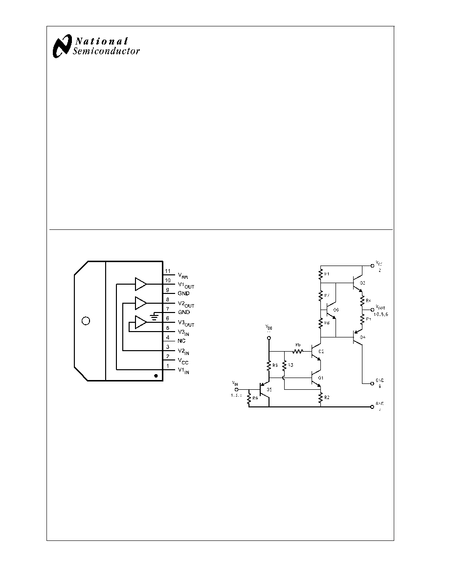
Connection Diagram
Schematic Diagram
20114801
FIGURE 1. Top View
Order Number LM2423TE
See NS Package Number TE11B NOPB
Available only with lead free plating
20114802
FIGURE 2. Simplified Schematic Diagram
(One Channel)
July 2004
LM2423
220V
Monolithic
T
riple
Channel
15
MHz
CRT
DTV
Driver
© 2004 National Semiconductor Corporation
DS201148
www.national.com
Absolute Maximum Ratings
(Notes 1,
3)
If Military/Aerospace specified devices are required,
please contact the National Semiconductor Sales Office/
Distributors for availability and specifications.
Supply Voltage (V
CC
)
+250V
Bias Voltage (V
BB
)
+16V
Input Voltage (V
IN
)
-0.5V to V
BB
+0.5V
Storage Temperature Range (T
STG
)
-65∞C to +150∞C
Lead Temperature
(Soldering,
<
10 sec.)
300∞C
ESD Tolerance,
Human Body Model
2 kV
Machine Model
200V
Junction Temperature
150∞C
JC
(typ)
2.2∞C/W
Operating Ratings
(Note 2)
V
CC
+100V to +230V
V
BB
+7V to +13V
V
IN
+0V to +5V
V
OUT
+40V to +215V
Case Temperature
110∞C
Do not operate the part without a heat sink.
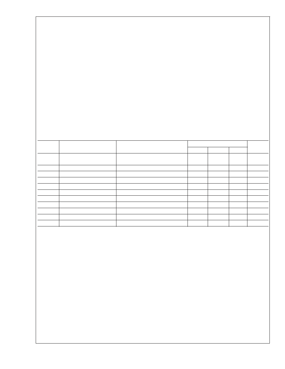
Electrical Characteristics
(See Figure 2 for Test Circuit) Unless otherwise noted: V
CC
= +220V, V
BB
= +12V, C
L
= 10 pF, T
C
= 50∞C. DC Tests: V
IN
=
+2.75V
DC
. AC Tests: Output = 130V
PP
(60V ≠ 190V) at 1 MHz.
Symbol
Parameter
Conditions
LM2423
Units
Min
Typ
Max
I
CC
Supply Current
No Input Signal, No Video Input, No
Output Load
14
21
28
mA
I
BB
Bias Current
9
15
22
mA
V
OUT, 1
DC Output Voltage
No AC Input Signal, V
IN
= 2.75V
DC
120
125
130
V
DC
V
OUT, 2
DC Output Voltage
No AC Input Signal, V
IN
= 1.25V
DC
200
205
210
V
DC
A
V
DC Voltage Gain
No AC Input Signal
-51
-54
-57
V/V
A
V
Gain Matching
(Note 4), No AC Input Signal
1.0
dB
LE
Linearity Error
(Notes 4, 5), No AC Input Signal
8
%
t
r
Rise Time, 60V to 190V
(Note 6), 10% to 90%
22
ns
+OS
Overshoot
8
%
t
f
Fall Time, 60V to 190V
(Note 6), 90% to 10%
21
ns
-OS
Overshoot
(Note 6)
4
%
Note 1: Absolute Maximum Ratings indicate limits beyond which damage to the device may occur.
Note 2: Operating ratings indicate conditions for which the device is functional, but do not guarantee specific performance limits. For guaranteed specifications and
test conditions, see the Electrical Characteristics. Datasheet min/max specification limits are guaranteed by design, test, or statistical analysis. The guaranteed
specifications apply only for the test conditions listed. Some performance characteristics may change when the device is not operated under the listed test
conditions.
Note 3: All voltages are measured with respect to GND, unless otherwise specified.
Note 4: Calculated value from Voltage Gain test on each channel.
Note 5: Linearity Error is the variation in DC gain from V
IN
= 1.15V to V
IN
= 4.35V.
Note 6: Input from signal generator: t
r
, t
f
<
1 ns.
LM2423
www.national.com
2

AC Test Circuit
Figure 3 shows a typical test circuit for evaluation of the LM2423. This circuit is designed to allow testing of the LM2423 in a 50
environment without the use of an expensive FET probe. The two 4990
resistors form a 400:1 divider with the 50 resistor and
the oscilloscope. A test point is included for easy use of an oscilloscope probe. The compensation capacitor is used to
compensate the network to achieve flat frequency response.
20114803
Note: 10 pF load includes parasitic capacitance.
FIGURE 3. Test Circuit (One Channel)
LM2423
www.national.com
3

Typical Performance Characteristics
(V
CC
= +220V
DC
, V
BB
= +12V
DC
, C
L
= 10 pF, V
OUT
= 130V
PP
(60V ≠ 190V), T
C
= 50∞C, Test Circuit -- Figure 3 unless otherwise specified)
20114804
FIGURE 4. V
OUT
vs V
IN
20114805
FIGURE 5. LM2423 Pulse Response
20114806
FIGURE 6. Bandwidth
20114807
FIGURE 7. Speed vs Load Capacitance
20114808
FIGURE 8. Speed vs Offset
20114809
FIGURE 9. Speed vs Case Temperature
LM2423
www.national.com
4
Typical Performance Characteristics
(V
CC
= +220V
DC
, V
BB
= +12V
DC
, C
L
= 10 pF, V
OUT
= 130V
PP
(60V ≠ 190V), T
C
= 60∞C, Test Circuit -- Figure 3 unless otherwise specified)
201148010
FIGURE 10. Power Dissipation vs Frequency
201148011
FIGURE 11. Safe Operating Area
201148012
FIGURE 12. LM2423 Cathode Response
LM2423
www.national.com
5