LM2432
220V Monolithic Single Channel 37 MHz HDTV CRT
Driver
General Description
The LM2432 is a single channel high voltage CRT driver
circuit designed for use in Rear-Projection and Direct-View
HDTV applications. The IC contains a high input impedance,
wide band amplifier which can be DC coupled to a cathode
of a CRT. The amplifier has its gain internally set to -53 and
can drive CRT capacitive loads as well as resistive loads
present in other applications, limited only by the package's
power dissipation.
The IC is packaged in a staggered 7-lead TO-220 molded
plastic power package designed specifically to meet high
voltage spacing requirements. See the section "Power Dis-
sipation and Heatsink Calculation" for more information.
Features
n
37 MHz bandwith at 110V
PP
output swing
n
0V to 4V input range
n
Greater than 130V
PP
output swing capability
n
IK Current Output (Pin 5) for IK feedback systems
n
Stable with 020 pF capacitive loads and inductive
peaking networks
Applications
n
For Rear-Projection and Direct-View DC coupled CRT
applications using up to 720p and 1080i HDTV formats
n
Compatible with RGB video processors with IK feedback
for automatic cathode calibration
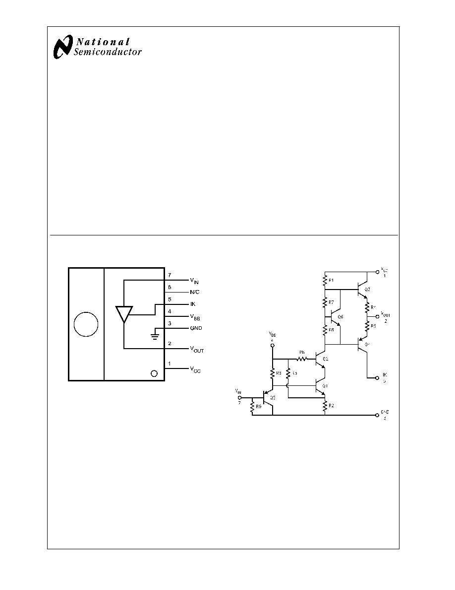
Pinout Diagram
Schematic Diagram
20137702
Note: Tab is at GND. Pin 6 is not connected (N/C) internally.
Top View
Order Number LM2432TE
FIGURE 1. Simplified Connection and Pinout Diagram
20137701
FIGURE 2. Simplified Schematic Diagram
September 2005
LM2432
220V
Monolithic
Single
Channel
37
MHz
HDTV
CRT
Driver
© 2005 National Semiconductor Corporation
DS201377
www.national.com
Absolute Maximum Ratings
(Notes 1,
3)
If Military/Aerospace specified devices are required,
please contact the National Semiconductor Sales Office/
Distributors for availability and specifications.
Supply Voltage (V
CC
)
+250V
Bias Voltage (V
BB
)
+16V
Input Voltage (V
IN
)
-0.5V to V
BB
+0.5V
IK Voltage (V
IK
)
-0.5V to +16V
Storage Temperature Range (T
STG
)
-65°C to +150°C
Lead Temperature
(Soldering,
<
10 sec.)
300°C
ESD Tolerance,
Human Body Model
2 kV
Machine Model
200V
Junction Temperature
150°C
JC
(typ)
4.5°C/W
Operating Ranges
(Note 2)
V
CC
+130V to +230V
V
BB
+7V to +13V
V
IN
0V to +4.25V
V
IK
0V to V
BB
+1V
V
OUT
+40V to V
CC
5V
Case Temperature
See Figure 11. Derate power for
T
C
above 110°C.
Do not operate the part without a heat sink.
Electrical Characteristics
(See Figure 3 for Test Circuit)
Unless otherwise noted: V
CC
= +220V, V
BB
= +12V, C
L
= 10 pF, T
C
= 40°C.
DC Tests: V
IN
= 2.75V
DC
AC Tests: Output = 110V
PP
(80V - 190V) at 1 MHz
Symbol
Parameter
Conditions
LM2432
Units
Min
Typical
Max
I
CC
Supply Current
No AC Input Signal, No Output Load
12
17
mA
I
BB
Bias Current
8
11
mA
V
OUT, 1
DC Output Voltage
No AC Input Signal, V
IN
= 2.75V
DC
121
126
131
V
DC
V
OUT, 2
DC Output Voltage
No AC Input Signal, V
IN
= 1.25V
DC
199
204
209
V
DC
A
V
DC Voltage Gain
No AC Input Signal
50
53
56
LE
Linearity Error
(Note 4), No AC Input Signal
5
%
t
R
Rise Time
(Note 5), 10% to 90%
10
ns
+OS
Overshoot
(Note 5)
21
%
t
F
Fall Time
(Note 5), 90% to 10%
8
ns
OS
Overshoot
(Note 5)
8
%
IK
ERROR
IK Current Output Error
(Notes 6, 7), V
CC
= 210V, V
OUT
=
150V
DC
11
0
+11
µA
Note 1: Absolute Maximum Ratings indicate limits beyond which damage to the device may occur.
Note 2: Operating ratings indicate conditions for which the device is functional, but do not guarantee specific performance limits. For guaranteed specifications and
test conditions, see the Electrical Characteristics. Datasheet min/max specification limits are guaranteed by design, test, or statistical analysis. The guaranteed
specifications apply only for the test conditions listed. Some performance characteristics may change when the device is not operated under the listed test
conditions.
Note 3: All voltages are measured with respect to GND, unless otherwise specified.
Note 4: Linearity Error is the variation in DC gain from V
IN
= 1.15V to V
IN
= 4.35V.
Note 5: Input from signal generator: t
r
, t
f
<
2 ns. Slower inputs to the LM2432 will change the transient response characteristics and reduce power dissipation.
Note 6: IK
ERROR
= I
K
I
OUT
, where I
K
is the IK current output from pin 5 (IK) and I
OUT
is the cathode current into pin 2 (V
OUT
). I
K
is calculated by measuring V
IK
across a known resistor value between pin 5 and GND.
Note 7: Refer to the RGB Video Processor data sheet for IK leakage compensation, feedback operation, and adjustment range information.
LM2432
www.national.com
2
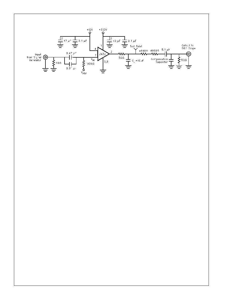
AC Test Circuit
Figure 3 shows a typical test circuit for evaluation of the LM2432. This circuit was designed to test the transient response of the
LM2432 in a 50
environment without the use of an expensive FET probe. On the input side, a 50 pulse generator output can
be AC coupled and biased with an external supply via the V
ADJ
input. On the output side, the two 4990
resistors form a 400:1
divider with the 50
resistor and the oscilloscope. A test point can be included for easy use of an oscilloscope probe. A
compensation capacitor can be used to compensate the network to achieve a flat frequency response.
20137703
Note: 10pF load includes parasitic capacitance.
FIGURE 3. Test Circuit
LM2432
www.national.com
3
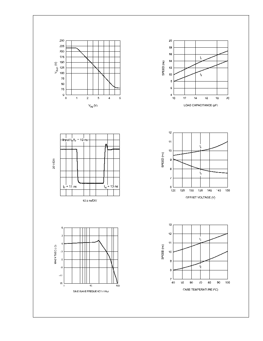
Typical Performance Characteristics
(V
CC
= +220V, V
BB
= +12V, C
L
= 10 pF, V
OUT
= 110V
PP
(80V
- 190V), Test Circuit - Figure 3, unless otherwise specified)
20137704
FIGURE 4. V
OUT
vs V
IN
20137723
FIGURE 5. LM2432 Pulse Response
20137720
FIGURE 6. Bandwidth
20137705
FIGURE 7. Speed vs Load Capacitance
20137708
FIGURE 8. Speed vs Offset
20137709
FIGURE 9. Speed vs Case Temperature
LM2432
www.national.com
4
Typical Performance Characteristics
(V
CC
= +220V, V
BB
= +12V, C
L
= 10 pF, V
OUT
= 110V
PP
(80V
- 190V), Test Circuit - Figure 3, unless otherwise specified) (Continued)
20137707
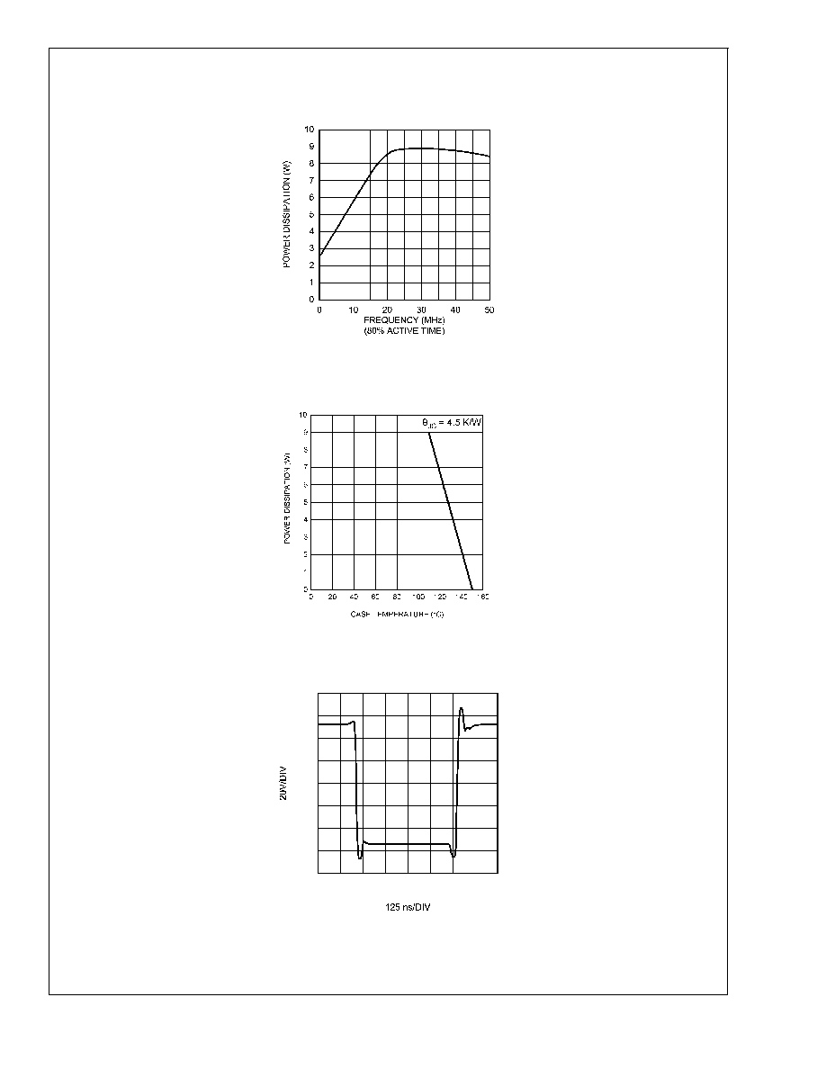
FIGURE 10. Power Dissipation vs Frequency
20137721
FIGURE 11. Power Derating Curve
20137719
FIGURE 12. Cathode Pulse Response
LM2432
www.national.com
5