LM2450
220V Monolithic Triple Channel 7 MHz DC Coupled CRT
DTV Driver
General Description
The LM2450 is a triple channel high voltage DC coupled
CRT driver circuit designed for use in DTV applications. The
IC contains three high input impedance, wide band amplifi-
ers which directly drive the RGB cathodes of a CRT. Each
amplifier has a summing input where the DC level of the
output is controlled by a low voltage DC input voltage. Nor-
mally the DC input voltage is from a DAC. Each channel has
its gain internally set to -54 and can drive CRT capacitive
loads as well as resistive loads present in other applications,
limited only by the package's power dissipation.
The IC is packaged in a 15-lead TO-247 molded plastic
power package designed specifically to meet high voltage
spacing requirements. See Thermal Considerations section.
Features
n
7 MHz bandwidth
n
100V black level adjustment range using 0V to 5V input
n
Current output for IK feedback systems
n
Greater than 130V
P-P
output swing capability
n
0V to 5V input voltage range
n
Stable with 0 pF20 pF capacitive loads and inductive
peaking networks
n
Convenient TO-247 staggered thin lead package style
Applications
n
DC coupled DTV applications using the 480p format as
well as standard NTSC and PAL formats.
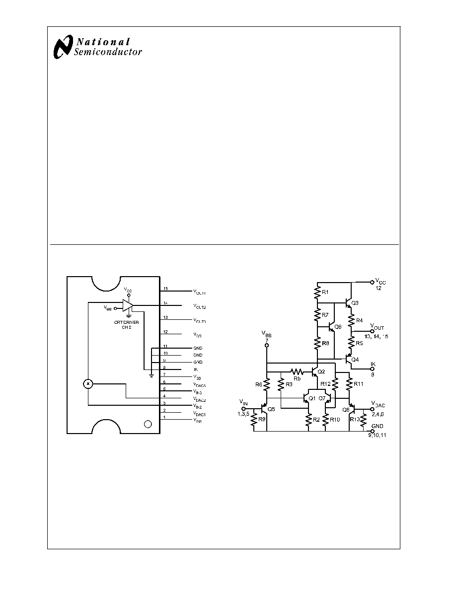
Connection Diagram
Schematic Diagram
20144301
FIGURE 1. Top View
Order Number LM2450TB
See NS Package Number TB15A
20144302
FIGURE 2. Simplified Schematic Diagram
(One Channel)
December 2005
LM2450
220V
Monolithic
T
riple
Channel
7
MHz
DC
Coupled
CRT
DTV
Driver
© 2005 National Semiconductor Corporation
DS201443
www.national.com
Absolute Maximum Ratings
(Notes 1,
3)
If Military/Aerospace specified devices are required,
please contact the National Semiconductor Sales Office/
Distributors for availability and specifications.
Supply Voltage (V
CC
)
+250V
Bias Voltage (V
BB
)
+16V
Input Voltage (V
IN
)
-0.5V to V
BB
+0.5V
Storage Temperature Range (T
STG
)
-65°C to +150°C
Lead Temperature
(Soldering,
<
10 sec.)
300°C
ESD Tolerance,
Human Body Model
2 kV
Machine Model
200V
Junction Temperature
150°C
JC
(typ)
4.0°C/W
Operating Ratings
(Note 2)
V
CC
+100V to +230V
V
BB
+7V to +13V
V
IN
+0V to +5V
V
OUT
+40V to +215V
Case Temperature
(10W max power)
110°C
Do not operate the part without a heat sink and thermal
grease. Heat sink must have a maximum thermal
resistance 5.4 °C/W. (Note 7)
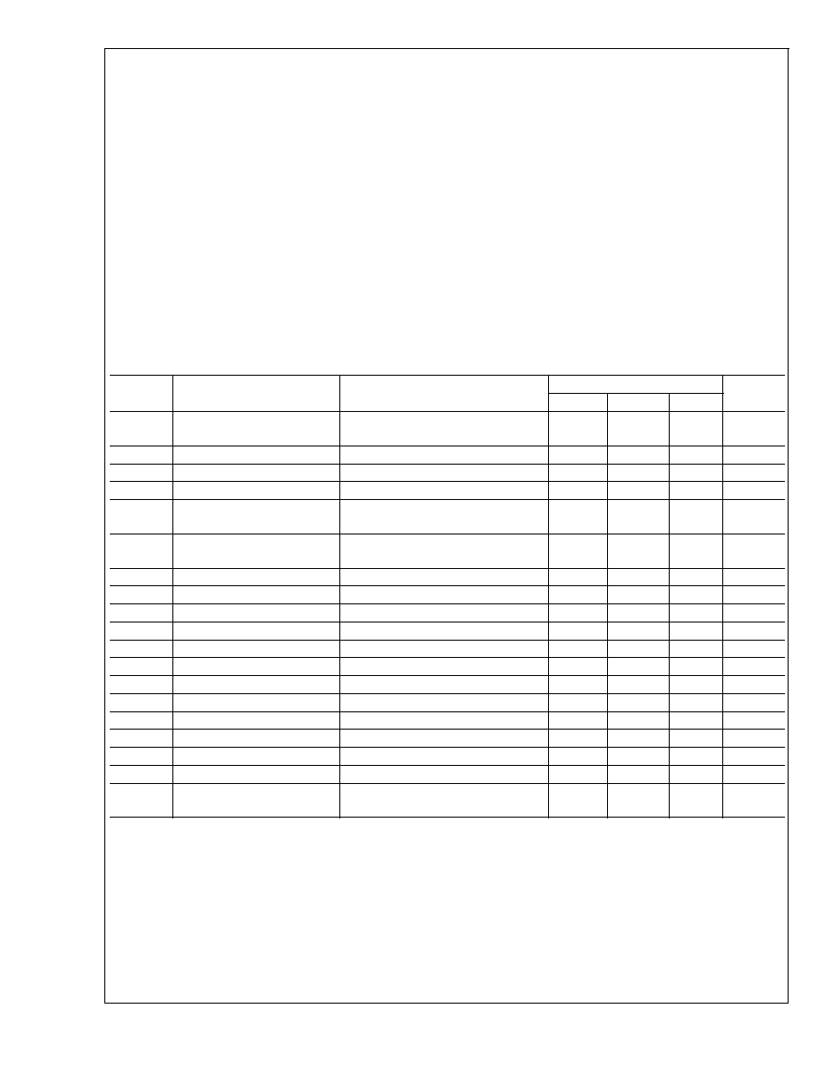
Electrical Characteristics
(See Figure 3 for Test Circuit). Unless otherwise noted: V
CC
= +220V, V
BB
= +12V, V
DAC
= +0.5V, C
L
= 10 pF, T
C
= 50°C. DC
Tests: V
IN
= +2.7V
DC
. AC Tests: Output = 130V
PP
(60V 190V) at 1 MHz.
Symbol
Parameter
Conditions
LM2450
Units
Min
Typ
Max
I
CC
Supply Current
No Input Signal, No Video Input, No
Output Load
10
18
25
mA
I
BB
Bias Current
18
26
34
mA
V
OUT, 1
DC Output Voltage
No AC Input Signal, V
IN
= 2.7V
DC
122
127
132
V
DC
V
OUT, 2
DC Output Voltage
No AC Input Signal, V
IN
= 1.2V
DC
200
205
210
V
DC
V
OUT, 3
DC Output Voltage
No AC Input Signal, V
IN
= 1.2V
DC
,
V
DAC
= 1.2V
DC
192
198
204
V
DC
V
OUT, 4
DC Output Voltage
No AC Input Signal, V
IN
= 1.2V
DC
,
V
DAC
= 2.7V
DC
154
160
166
V
DC
A
V
DC Voltage Gain
No AC Input Signal
-51
-54
-57
V/V
A
DAC
DAC Input DC Voltage Gain
No AC Input Signal
-23
-26
-29
V/V
A
V
Gain Matching
(Note 4), No AC Input Signal
1.0
dB
LE
Linearity Error
(Notes 4, 5), No AC Input Signal
8
%
t
r
Rise Time
(Note 6), 10% to 90%
49
ns
+OS
Overshoot
2
%
t
f
Fall Time
(Note 6), 90% to 10%
52
ns
-OS
Overshoot
(Note 6)
1
%
BW
L
Large Signal Bandwidth
V
OUT AC
= 130 V
P-P
, V
OUT DC
= 125 V
7
MHz
BW
M
Medium Signal Bandwidth
V
OUT AC
= 100 V
P-P
, V
OUT DC
= 125 V
8
MHz
BW
S
Small Signal Bandwidth
V
OUT AC
= 60 V
P-P
, V
OUT DC
= 125 V
9
MHz
Ik
ERROR
Current Output Error
Output Current = 0 µA to 200 µA
-52
0
52
µA
Ik
ERROR
Current Output Difference
Between Channels
Output Current = 0 µA to 200 µA
0
NA
32
µA
Note 1: Absolute Maximum Ratings indicate limits beyond which damage to the device may occur.
Note 2: Operating ratings indicate conditions for which the device is functional, but do not guarantee specific performance limits. For guaranteed specifications and
test conditions, see the Electrical Characteristics. Datasheet min/max specification limits are guaranteed by design, test, or statistical analysis. The guaranteed
specifications apply only for the test conditions listed. Some performance characteristics may change when the device is not operated under the listed test
conditions.
Note 3: All voltages are measured with respect to GND, unless otherwise specified.
Note 4: Calculated value from Voltage Gain test on each channel.
Note 5: Linearity Error is the variation in DC gain from V
IN
= 1.10V to V
IN
= 4.30V.
Note 6: Input from signal generator: t
r
, t
f
<
10 ns.
Note 7: Running the 1 MHz to 30 MHz test pattern at 1080i this part will dissipate approximately 9.2 W. This is the commonly accepted test pattern that is
representative of the worst case high frequency content for normal television viewing. This is the pattern used to estimate the worst case power dissipation of the
LM2450 in its normal application. It is recommended to use a heat sink with a thermal resistance of 5.4°C/W or better.
LM2450
www.national.com
2
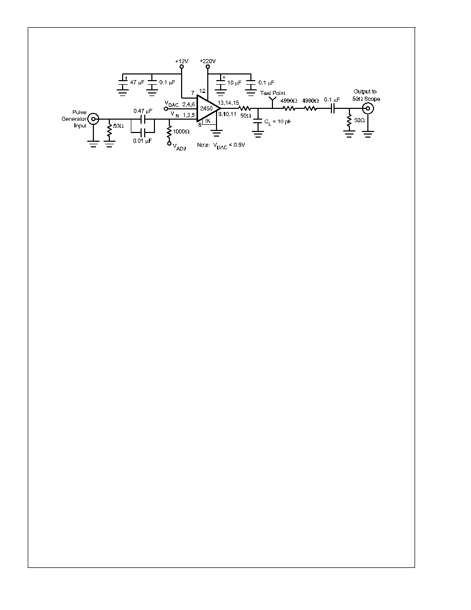
AC Test Circuit
Figure 3 shows a typical test circuit for evaluation of the LM2450. This circuit is designed to allow testing of the LM2450 in a 50
environment without the use of an expensive FET probe. The two 4990
resistors form a 400:1 divider with the 50 resistor and
the oscilloscope. A test point is included for easy use of an oscilloscope probe. The compensation capacitor is used to
compensate the network to achieve flat frequency response.
20144303
Note: 10 pF load includes parasitic capacitance.
FIGURE 3. Test Circuit (One Channel)
LM2450
www.national.com
3
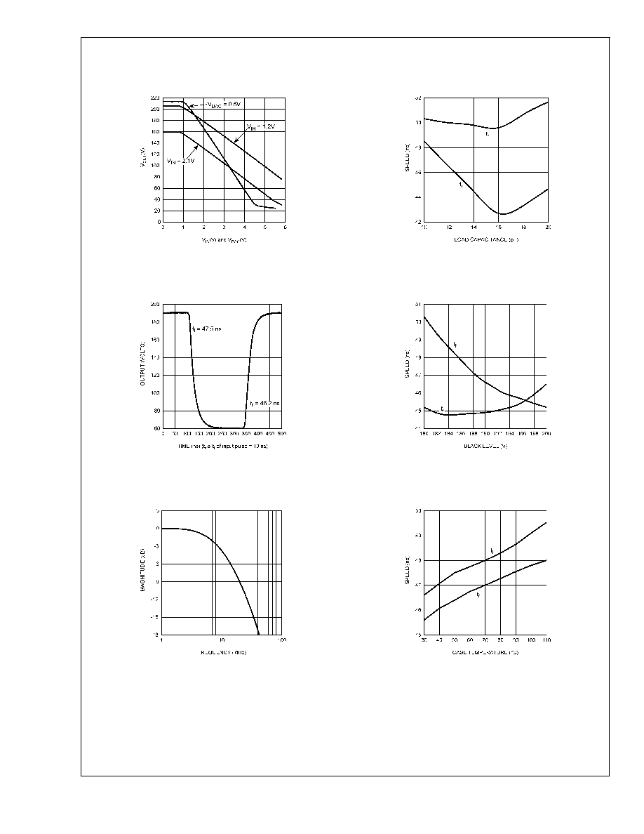
Typical Performance Characteristics
(V
CC
= +220V
DC
, V
BB
= +12V
DC
, C
L
= 10 pF, V
OUT
= 130V
PP
(60V 190V), T
C
= 50°C, Test Circuit -- Figure 3 unless otherwise specified)
20144304
FIGURE 4. V
OUT
vs V
IN
20144305
FIGURE 5. LM2450 Pulse Response
20144306
FIGURE 6. Bandwidth
20144307
FIGURE 7. Speed vs Load Capacitance
20144308
FIGURE 8. Speed vs Offset
20144309
FIGURE 9. Speed vs Case Temperature
LM2450
www.national.com
4
Typical Performance Characteristics
(V
CC
= +220V
DC
, V
BB
= +12V
DC
, C
L
= 10 pF, V
OUT
= 130V
PP
(60V 190V), T
C
= 50°C, Test Circuit -- Figure 3 unless otherwise specified)
20144310
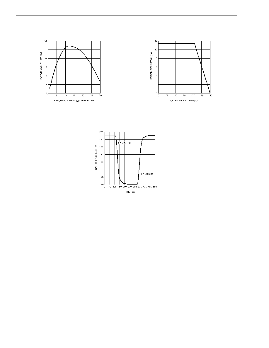
FIGURE 10. Power Dissipation vs Frequency
20144311
FIGURE 11. Safe Operating Area
20144312
FIGURE 12. LM2450 Cathode Response
LM2450
www.national.com
5