 | –≠–ª–µ–∫—Ç—Ä–æ–Ω–Ω—ã–π –∫–æ–º–ø–æ–Ω–µ–Ω—Ç: LM2465TA | –°–∫–∞—á–∞—Ç—å:  PDF PDF  ZIP ZIP |

LM2465
Monolithic Triple 5.5 ns High Gain CRT Driver
General Description
The LM2465 is an integrated high voltage CRT driver circuit
designed for use in color monitor applications. The IC
contains three high input impedance, wide band amplifiers
which directly drive the RGB cathodes of a CRT. Each
channel has its gain internally set to -20 and can drive CRT
capacitive loads as well as resistive loads present in other
applications, limited only by the package's power dissipation.
The IC is packaged in an industry standard 9-lead TO-220
molded plastic package.
Features
n
Higher gain to match LM126X CMOS preamplifiers
n
0V to 3.75V input range
n
Stable with 0≠20 pF capacitive loads and inductive
peaking networks
n
Same pinout as LM2467/8/9, maintaining the standard
LM243X Family pinout for easy PCB layout
n
Convenient TO-220 staggered lead package style
Applications
n
Up to 1280 x 1024 at 75Hz
n
Pixel clock frequencies up to 135 MHz
n
Monitors using video blanking
Schematic and Connection Diagrams
DS200190-1
FIGURE 1. Simplified Schematic Diagram
(One Channel)
DS200190-2
Note: Tab is at GND
Top View
Order Number LM2465TA
March 2001
LM2465
Monolithic
T
riple
5.5
ns
High
Gain
CRT
Driver
© 2001 National Semiconductor Corporation
DS200190
www.national.com

Absolute Maximum Ratings
(Notes 1, 3)
If Military/Aerospace specified devices are required,
please contact the National Semiconductor Sales
Office/Distributors for availability and specifications.
Supply Voltage (V
CC
)
+90V
Bias Voltage (V
BB
)
+16V
Input Voltage (V
IN
)
0V to 4.5V
Storage Temperature Range (T
STG
)
-65∞C to +150∞C
Lead Temperature
(Soldering,
<
10 sec.)
300∞C
ESD Tolerance, Human Body Model
2 kV
Machine Model
250V
Operating Ranges
(Note 2)
V
CC
+60V to +85V
V
BB
+8V to +15V
V
IN
+0V to +3.75V
V
OUT
+15V to +75V
Case Temperature
-20∞C to +100∞C
Do not operate the part without a heat sink.
Electrical Characteristics
(See
Figure 2 for Test Circuit)
Unless otherwise noted: V
CC
= +80V, V
BB
= +12V, C
L
= 8 pF, T
C
= 50∞C
DC Tests: V
IN
= 2.25VDC
AC Tests: Output = 40V
PP
(25V - 65V) at 1MHz
Symbol
Parameter
Conditions
LM2465
Units
Min
Typical
Max
I
CC
Supply Current
All Three Channels, No Input Signal,
No Output Load
36
44
mA
I
BB
Bias Current
All Three Channels
20
24
mA
V
OUT
DC Output Voltage
No AC Input Signal, V
IN
= 1.25V
62
65
68
V
DC
A
V
DC Voltage Gain
No AC Input Signal
-18
-20
-22
A
V
Gain Matching
(Note 4), No AC Input Signal
1.0
dB
LE
Linearity Error
(Notes 4, 5), No AC Input Signal
5
%
t
R
Rise Time
(Note 6), 10% to 90%
5.5
ns
t
F
Fall Time
(Note 6), 90% to 10%
6.0
ns
OS
Overshoot
(Note 6)
3
%
Note 1: Absolute Maximum Ratings indicate limits beyond which damage to the device may occur.
Note 2: Operating ratings indicate conditions for which the device is functional, but do not guarantee specific performance limits. For guaranteed specifications and
test conditions, see the Electrical Characteristics. The guaranteed specifications apply only for the test conditions listed. Some performance characteristics may
change when the device is not operated under the listed test conditions.
Note 3: All voltages are measured with respect to GND, unless otherwise specified.
Note 4: Calculated value from Voltage Gain test on each channel.
Note 5: Linearity Error is the variation in dc gain from V
IN
= 1.0V to V
IN
= 3.5V.
Note 6: Input from signal generator: t
r
, t
f
<
1 ns.
LM2465
www.national.com
2

AC Test Circuit
Figure 2 shows a typical test circuit for evaluation of the LM2465. This circuit is designed to allow testing of the LM2465 in a 50
environment without the use of an expensive FET probe. The two 2490
resistors form a 200:1 divider with the 50
resistor and
the oscilloscope. A test point is included for easy use of an oscilloscope probe.The compensation capacitor is used to
compensate the stray capacitance of the two 2490
resistors to achieve flat frequency response.
DS200190-3
Note: 8 pF load includes parasitic capacitance.
FIGURE 2. Test Circuit (One Channel)
LM2465
www.national.com
3
Typical Performance Characteristics
(V
CC
= +80V
DC
, V
BB
= +12V
DC
, C
L
= 8pF, V
OUT
= 40V
PP
(25V-65V), Test Circuit -
Figure 2 unless otherwise specified)
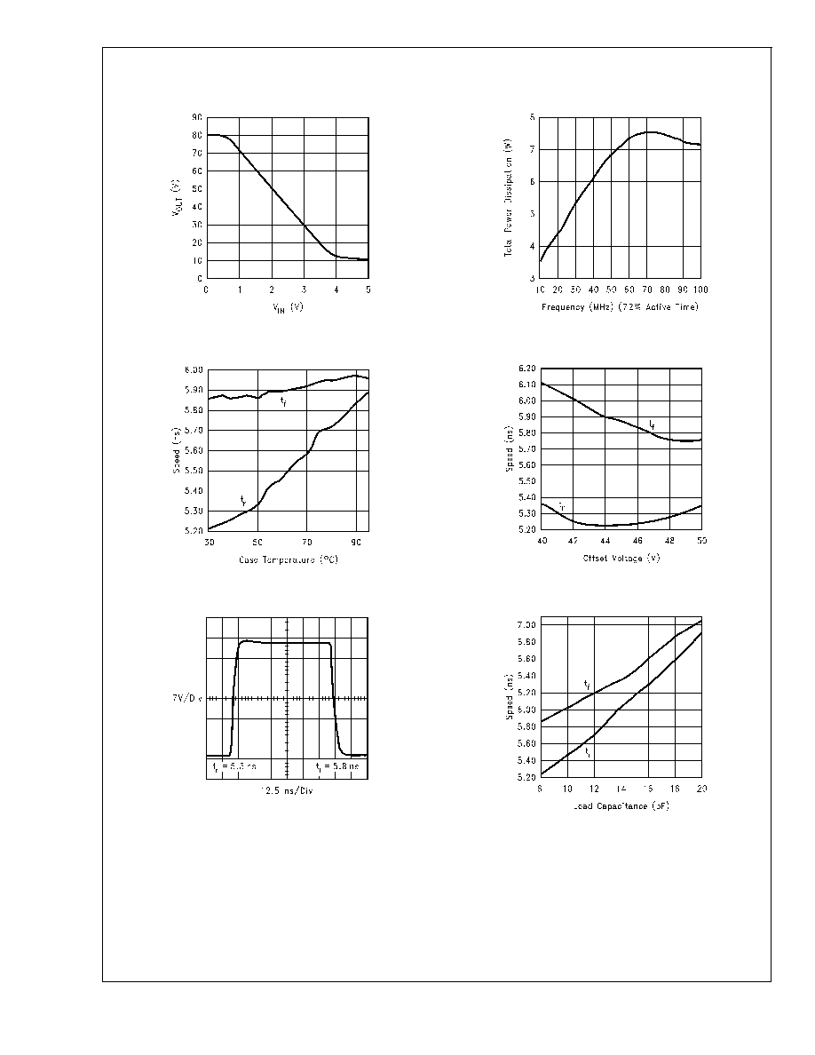
DS200190-4
FIGURE 3. V
OUT
vs V
IN
DS200190-5
FIGURE 4. Speed vs Temperature
DS200190-6
FIGURE 5. LM2465 Pulse Response
DS200190-7
FIGURE 6. Power Dissipation vs Frequency
DS200190-8
FIGURE 7. Speed vs Offset
DS200190-9
FIGURE 8. Speed vs Load Capacitance
LM2465
www.national.com
4

Theory of Operation
The LM2465 is a high voltage monolithic three channel CRT
driver suitable for high resolution display applications. The
LM2465 operates with 80V and 12V power supplies. The
part is housed in the industry standard 9-lead TO-220
molded plastic power package.
The circuit diagram of the LM2465 is shown in
Figure 1. The
PNP emitter follower, Q5, provides input buffering. Q1 and
Q2 form a fixed gain cascode amplifier with resistors R1 and
R2 setting the gain at -20. Emitter followers Q3 and Q4
isolate
the
high
output
impedance
of
the
amplifier,
decreasing the sensitivity of the device to changes in load
capacitance. Q6 provides biasing to the output emitter
follower stage to reduce crossover distortion at low signal
levels.
Figure 2 shows a typical test circuit for evaluation of the
LM2465. This circuit is designed to allow testing of the
LM2465 in a 50
environment without the use of an
expensive FET probe. In this test circuit, two low inductance
resistors in series totaling 4.95k
form a 200:1 wideband,
low capacitance probe when connected to a 50
coaxial
cable and a 50
load (such as a 50
oscilloscope input).
The input signal from the generator is ac coupled to the base
of Q5.
Application Hints
INTRODUCTION
National Semiconductor (NSC) is committed to provide
application information that assists our customers in
obtaining the best performance possible from our products.
The following information is provided in order to support this
commitment. The reader should be aware that the
optimization of performance was done using a specific
printed circuit board designed at NSC. Variations in
performance can be realized due to physical changes in the
printed circuit board and the application. Therefore, the
designer should know that component value changes may
be required in order to optimize performance in a given
application. The values shown in this document can be used
as a starting point for evaluation purposes. When working
with high bandwidth circuits, good layout practices are also
critical to achieving maximum performance.
IMPORTANT INFORMATION
The LM2465 performance is targeted for the 17" and low end
19" monitor market with resolutions up to 1280 X 1024 and a
75Hz refresh rate. It is designed to be a replacement for
discrete CRT drivers. The application circuits shown in this
document to optimize performance and to protect against
damage from CRT arcover are designed specifically for the
LM2465. If another member of the LM246X family is used,
please refer to its datasheet.
POWER SUPPLY BYPASS
Since the LM2465 is a wide bandwidth amplifier, proper
power supply bypassing is critical for optimum performance.
Improper power supply bypassing can result in large
overshoot, ringing or oscillation. A 0.1 µF capacitor should be
connected from the supply pin, V
CC
and V
BB
, to ground, as
close to the LM2465 as is practical. Additionally, a 47µF or
larger electrolytic capacitor should be connected from both
supply pins to ground reasonably close to the LM2465.
ARC PROTECTION
During
normal
CRT
operation,
internal
arcing
may
occasionally occur. Spark gaps, in the range of 200V,
connected from the CRT cathodes to CRT ground will limit
the maximum voltage, but to a value that is much higher than
allowable on the LM2465. This fast, high voltage, high
energy pulse can damage the LM2465 output stage. The
application circuit shown in
Figure 9 is designed to help
clamp the voltage at the output of the LM2465 to a safe level.
The clamp diodes, D1 and D2, should have a fast transient
response, high peak current rating, low series impedance
and low shunt capacitance. FDH400 or equivalent diodes
are recommended. Do not use 1N4148 diodes for the clamp
diodes. D1 and D2 should have short, low impedance
connections to V
CC
and ground respectively. The cathode of
D1 should be located very close to a separately decoupled
bypass capacitor (C3 in
Figure 9). The ground connection of
D2 and the decoupling capacitor should be very close to the
LM2465 ground. This will significantly reduce the high
frequency voltage transients that the LM2465 would be
subjected to during an arcover condition. Resistor R2 limits
the arcover current that is seen by the diodes while R1 limits
the current into the LM2465 as well as the voltage stress at
the outputs of the device. R2 should be a
1
/
2
W solid carbon
type resistor. R1 can be a
1
/
4
W metal or carbon film type
resistor. Having large value resistors for R1 and R2 would be
desirable, but this has the effect of increasing rise and fall
times. Inductor L1 is critical to reduce the initial high
frequency voltage levels that the LM2465 would be
subjected to. The inductor will not only help protect the
device but it will also help optimize rise and fall times as well
as minimize EMI. For proper arc protection, it is important to
not omit any of the arc protection components shown in
Figure 9.
LM2465
www.national.com
5