 | –≠–ª–µ–∫—Ç—Ä–æ–Ω–Ω—ã–π –∫–æ–º–ø–æ–Ω–µ–Ω—Ç: LM2485 | –°–∫–∞—á–∞—Ç—å:  PDF PDF  ZIP ZIP |
LM2485
220V Triple Bias Clamp with G1 Blank Amplifier
General Description
The LM2485 is a triple channel clamp amplifier used to DC
restore the AC coupled outputs of a DTV CRT driver and for
cut-off adjustment. The LM2485 also has an integrated
blanking amplifier that can be used to drive the G1 grid of a
CRT negative for vertical retrace blanking. The blanking
output has a selectable pulse amplitude of either 20V
P-P
or
40V
P-P
via the Pin 13 option. The blanking input pulse can
be generated from a vertical flyback pulse or by a microcon-
troller.
The LM2485 can operate with a V
CC
supply of up to 220V
and a V
BB
supply of either 8V or 12V. This V
BB
option,
selectable via the Pin 12 option, ensures the LM2485 is
compatible with any National Semiconductor DTV CRT
driver sharing the same operating voltages in the applica-
tion.
The IC is packaged in an industry standard 24-lead molded
plastic dual-in-line package to meet high voltage spacing
requirements.
Features
n
V
CC
capable of up to 220V
n
V
BB
selectable to 8V or 12V via Pin 12 option
n
Wide bias output voltage range of over 100V
n
Inverted output pulse suitable for G1 blanking,
selectable to 20V
P-P
or 40V
P-P
via Pin 13 option
Applications
n
AC coupled CRT applications using DTV formats up to
1080i
n
Well-matched to the NSC LM12XX Family of
Preamplifiers and LM242X/3X/5X Family of DTV CRT
Drivers
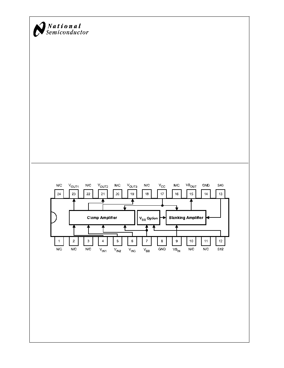
Pinout and Internal Block Diagram
20103433
FIGURE 1. Top View
Order Number LM2485NA
See NS Package Number N24C
December 2004
LM2485
220V
T
riple
Bias
Clamp
with
G1
Blank
Amplifier
© 2004 National Semiconductor Corporation
DS201034
www.national.com
Absolute Maximum Ratings
(Notes 1,
3)
If Military/Aerospace specified devices are required,
please contact the National Semiconductor Sales Office/
Distributors for availability and specifications.
Supply Voltage, V
CC
250V
Bias Voltage, V
BB
15V
Input Voltage, V
IN
-0.5V to +6.5V
Blanking Input Voltage, VB
IN
-0.5V to +6.5V
Storage Temperature Range, T
STG
-65∞C to +150∞C
Lead Temperature (Soldering,
<
10sec.)
300∞C
ESD Tolerance
Human Body Model
2 kV
Machine Model
200V
Max Junction Temperature
150∞C
JA
(Max at 0 LFPM)
68∞C/W
Operating Ranges
(Note 3)
V
CC
170V to 230V
V
BB
(Pin 12 floated)
7.5V to 8.5V
V
BB
(Pin 12 grounded)
11.5V to 12.5V
V
IN
0V to 5V
V
OUT
105V to 215V
VB
IN
0V to 5V
VB
OUT
(V
CC
= 220V)
40V to 80V
VB
OUT
(V
CC
= 180V)
25V to 65V
Ambient Temperature Range, T
A
-20∞C to T
AMAX
(Note 5)
Electrical Characteristics
(See Figure 2 and Figure 3 for Test Circuits)
Unless otherwise noted: V
CC
= 220V, V
BB
= 8V, V
IN
= 2.5V
DC
, T
A
= 20∞C, Pin 12 floated, Pin 13 grounded.
Symbol
Parameter
Conditions
Min
Typ
Max
Units
I
CC
Supply Current
All channels, not including pull-up
resistor currents
3.1
4.2
mA
I
BB≠8
Bias Supply Current
All channels, V
BB
= 8V
6.0
10.0
mA
I
BB≠12
Bias Supply Current
All channels, Pin 12 grounded,
V
BB
= 12V
9.0
13.0
mA
V
OUT
Clamp Output Voltage
170
175
180
V
DC
V
OUT-Range
Clamp Output Voltage
Range
V
IN-Range
= 1.5V to 4.5V
75
V
A
V
Clamp Output DC Voltage
Gain
1.0V
V
IN
5.0V
≠23
≠25
≠27
V/V
LE
Clamp Output Linearity
Error
(Note 4)
5
%
VB
OUT-High
Blanking Output High
Level
VB
IN
0.5V
80
V
DC
VB
OUT-Low1
Blanking Output Low
Level 1
VB
IN
4.5V, Pin 13 floated
60
V
DC
VB
OUT-Low2
Blanking Output Low
Level 2
VB
IN
4.5V
40
V
DC
t
R
Blanking Output Rise
Time
VB
IN
= 0V≠5V Logic Pulse at 8.6%
duty cycle (480p), VB
OUT
= 40V
P-P
(40V-80V)
2.0
us
t
F
Blanking Output Fall Time VB
IN
= 0V≠5V Logic Pulse at 8.6%
duty cycle (480p), VB
OUT
= 40V
P-P
(40V-80V)
4.5
us
Note 1: Absolute Maximum Ratings indicate limits beyond which damage to the device may occur.
Note 2: Operating Ratings indicate conditions for which the device is functional, but do not guarantee specific performance limits. For guaranteed specifications and
the test conditions, see the Electrical Characteristics. Datasheet min/max specification limits are guaranteed by design, test, or statistical analysis. The guaranteed
specifications apply only for the test conditions listed. Some performance characteristics may change when the device is not operated under the listed test
conditions.
Note 3: All voltages are measured with respect to GND, unless otherwise specified.
Note 4: Linearity Error is the variation in DC gain from V
IN
= 1.0V to 5.0V measured at the points 1.0V, 1.5V, 4.5V, and 5.0V.
Note 5: See Section THERMAL CONSIDERATIONS to calculate T
AMAX
.
LM2485
www.national.com
2
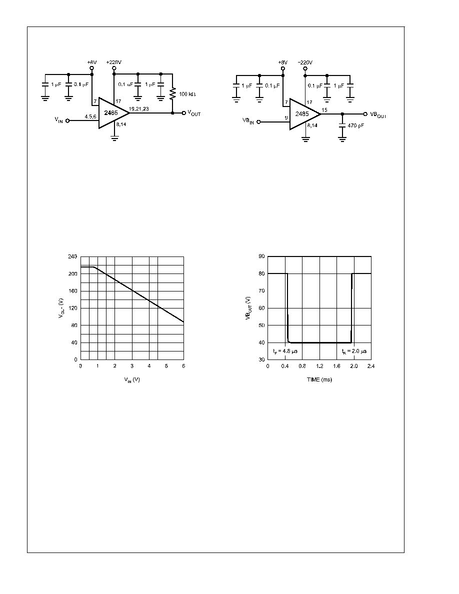
Test Circuits
Figure 2 shows the test circuit used to evaluate the LM2485 clamp amplifier. A high impedance voltmeter (
>
10M
) is used to
measure the DC voltages at the V
OUT
output pins. Figure 3 shows the test circuit used to evaluate the LM2485 blanking amplifier.
An oscilloscope and a scope probe are used to measure the pulse amplitude at the VB
OUT
output pin.
Typical Performance Characteristics
(V
CC
= 220V, V
BB
= 8V, VB
IN
= 0V≠5V Logic Pulse at 8.6% duty cycle, Pin 12 floated, Pin 13 grounded, Test Circuits - Figure 2
and Figure 3)
20103434
FIGURE 2. Clamp Amplifier Test Circuit
20103437
FIGURE 3. Blanking Amplifier Test Circuit
20103435
FIGURE 4. V
OUT
vs. V
IN
20103438
FIGURE 5. VB
OUT
(40V
P-P
)
LM2485
www.national.com
3

Theory of Operation
The pinout and internal block diagram of the LM2485 is
shown in Figure 1.
The LM2485 is a triple channel bias clamp amplifier used to
DC restore the AC coupled outputs of a DTV CRT driver and
for cut-off adjustment. The clamp circuit amplifies the DC
inputs, V
IN
, by the internally fixed gain of ≠25. Each DC
clamp output, V
OUT
, will require a pull-up resistor to V
CC
.
The clamp DC transfer function is shown in Figure 4.
The LM2485 also has an integrated blanking amplifier that
takes a positive-going 5V input pulse, VB
IN
, and outputs a
negative-going pulse, VB
OUT
, with a selectable amplitude of
either 20V
P-P
or 40V
P-P
via the Pin 13 (S40) option. If Pin 13
is floated, the VB
OUT
pulse amplitude is 20V
P-P
; if Pin 13 is
grounded, the amplitude is 40V
P-P
(see Figure 5). With a
simple clamp circuit, this inverted pulse can be used to drive
the G1 grid of a CRT negative to blank the horizontal retrace
lines during the vertical flyback period. The input pulse can
be generated from a vertical flyback pulse or by a microcon-
troller.
The LM2485 can operate with a V
CC
supply of up to 220V
and a selectable V
BB
supply of either 8V or 12V via the Pin
12 (S12) option. If Pin 12 is floated, then 8V is expected at
the V
BB
pin; if Pin 12 is grounded, then 12V is expected. This
V
BB
option ensures the LM2485 is compatible with any
National Semiconductor DTV CRT driver sharing the same
operating voltages in the application. Note that using a V
BB
supply of 12V will increase the input offset of the clamp
circuit, which would have the effect of shifting the DC trans-
fer function slightly to the right. Also, if the V
BB
option is
incorrectly matched to the actual V
BB
supply voltage, an
incorrect VB
OUT
amplitude will be produced. Therefore, it is
important to ensure that the appropriate V
BB
option is used
and the V
BB
supply is within the range stated in the Section
Operating Ranges .
Application Information
INTRODUCTION
National Semiconductor (NSC) is committed to provide ap-
plication information that assists our customers in obtaining
the best performance possible from our products. The fol-
lowing information is provided in order to support this com-
mitment. The reader should be aware that the optimization of
performance was done using a specific printed circuit board
designed at NSC. Variations in performance can be realized
due to physical changes in the printed circuit board and the
application. Therefore, the designer should know that com-
ponent value changes may be required in order to optimize
performance in a given application. The values shown in this
document can be used as a starting point for evaluation
purposes.
POWER SUPPLY BYPASS
The LM2485 should have proper power supply bypassing for
optimal arc protection and performance. A 0.1 µF capacitor
should be connected from each of the supply pins, V
CC
and
V
BB
, to ground, as close to the supply and ground pins as
possible. Additionally, a 1 µF electrolytic capacitor should be
connected from each supply to the LM2485 ground and
placed reasonably close to both supply pins.
ARC PROTECTION
During normal CRT operation, internal arcing may occasion-
ally occur. To protect the LM2485 against arcing, it is impor-
tant that the recommended applications circuit is used and
good layout practices are followed. Please refer to the Sec-
tion NSC Demonstration Board for a detailed example on arc
protection and PCB layout considerations.
THERMAL CONSIDERATIONS
Determining Maximum Power Dissipation and Ambient
Temperature
Power dissipation within an integrated circuit package is a
very important parameter. An incorrect maximum power dis-
sipation calculation may result in excessive thermal stress to
the device, affecting its reliability and performance. To esti-
mate the maximum power dissipation of the LM2485, the
following system parameters should be determined first.
∑
Maximum V
CC
and V
BB
supply voltages
∑
Average CRT cut-off voltages
∑
Maximum average beam currents
∑
Highest duty cycle
Once these parameters are known, the system designer can
then calculate the maximum ambient temperature surround-
ing the LM2485 without a heat sink. A small, low-cost heat
sink may be used if the calculated maximum ambient tem-
perature does not satisfy the worst-case operating tempera-
ture inside the TV.
The following example shows how to determine the maxi-
mum power dissipation and maximum ambient temperature
and assumes the recommended application circuit is used
(see Figure 6).
Example
The LM2485 uses 1.0W of static power from the 220V and
8V supplies, assuming the worst-case supply currents. If the
average CRT cut-off voltage of all channels is 180V and
each LM2485 output sinks a maximum average beam cur-
rent of 1.0 mA at 77% duty cycle (480p format) at the highest
brightness setting, the LM2485 will dissipate:
P
DISS
= P
STATIC
+ 3 x (V
CUT-OFF
x I
AVGMAX
) x
, or
P
DISS
= 1.0W + 3 x (180V x 1.0 mA) x 0.77 = 1.42W.
The maximum thermal resistance from junction-to-air,
JA
,
and maximum junction temperature, T
JMAX
, are stated in the
Section Absolute Maximum Ratings . Therefore, the maxi-
mum ambient temperature surrounding the LM2485 can be
calculated:
T
AMAX
= T
JMAX
- (P
DISS
x
JA
), or
T
AMAX
= 150∞C - (1.42W x 68∞C/W) = 53∞C.
TYPICAL APPLICATION
Used in conjunction with NSC's LM12XX Preamplifier and
LM24XX CRT Driver, a complete analog video solution from
the preamplifier input to the CRT cathode can be achieved.
The LM2485 can support any AC coupled DTV application
using formats up to 1080i with proper selection of a pream-
plifier and CRT drivers.
LM2485
www.national.com
4

NSC Demonstration Board
Figure 6 shows the recommended application schematic for
the NSC Demonstration Board that can be used to evaluate
the LM2423/LM2485 AC coupled solution in a Direct-View
CRT Digital TV application. Figure 7 shows the routing and
component placement on the NSC LM2423/LM2485 Dem-
onstration Board. This board provides a good example of a
PCB layout that was designed for robust arc protection and
optimal video performance.
PCB LAYOUT CONSIDERATIONS
Note that the NSC Demonstration Board complies with the
layout guidelines outlined below. For convenience, the com-
ponent names are shown in parenthesis to cross-reference
with the schematic and layout images provided.
Power Supplies and Grounds
∑
0.1uF bypass capacitors (C3 and C6) should be placed
very close to V
BB
and V
CC
of the LM2485. These capaci-
tors should have a short, direct return to the LM2485
ground.
∑
1uF electrolytic capacitors (C1 and C2) should also be
placed reasonably close to both supply pins.
∑
GND Pins 8 and 14 should connect to a solid ground
plane under the LM2485. The LM2485 ground plane
should connect directly to the CRT Driver ground at one
point (above C21). Do not connect the LM2485 ground
plane directly to CRT ground to protect the LM2485 from
arcing.
Inputs
∑
The LM2485 input traces should be routed away from all
output traces of the CRT Driver. This will help protect the
video preamplifier and LM2485 from high frequency,
large amplitude video coupling and potential damage
from arcing at the cathodes.
∑
If the LM2485 inputs are coming from the main board,
0.1uF capacitors (C4, C5, C7) should be placed at the
V
IN
pins of the input connector. If a LM12XX preamplifier
is placed on the neck board, these 0.1uF capacitors
should be placed very close to its DAC output pins to
protect it during arcing. In both cases, these capacitors
should be connected to the LM2485 ground and should
not be connected directly to CRT ground.
∑
1k
series resistors (R1, R3, R4) should be placed close
to the V
IN
pins and a small resistor may also be placed
close to the VB
IN
pin. These resistors will protect the
preamplifier in the event that the LM2485 fails.
Outputs
∑
1.5k
resistors (R6, R7, R8) and 0.1uF capacitors (C21,
C24, C25) should be placed near the V
OUT
pins to limit
the current and voltage surges on the outputs during an
arc event. These bypass capacitors should have a short,
direct return to the LM2485 ground.
∑
Because the clamp outputs carry DC, the clamp output
traces routed to each AC coupled video output can be
long. Avoid cutting a ground trace(s) simply to route
clamp output traces and use wire jumpers, if necessary.
∑
Clamp diodes (D3, D5, D6) and pull-up resistors (R20,
R23, R24) should be placed closest to the video output
traces to minimize the size of the video nodes and reduce
parasitic capacitance on the video outputs. The clamp
diodes must be 1SS83 or equivalent diodes; do not use
1N4148 type diodes. These diodes must have a fast
transient response, low shunt capacitance, low series
impedance, and a high peak current rating to clamp the
video output voltage to the V
CC
supply during an arc
event.
∑
0.1uF bypass capacitors (C46, C48, C9) should be
placed very close to the 1SS83 type arc protection diodes
(D1/D2, D4/D7, D8/D9) between V
CC
and ground. The
ground connection should have a short, direct path to
CRT ground. Therefore, arc currents shunted by the pro-
tection diodes can return to the CRT DAG (J6).
∑
300V spark gaps (S1, S2, S3, S4) are strongly recom-
mended and should be placed very close to the cathode
and G1 pins and grounded directly to the CRT ground
plane, so arc current can return to the nearby CRT DAG.
Spark gaps help to minimize voltage stress on the CRT
Driver and LM2485.
∑
If the G1 blanking feature is used, all G1 circuit compo-
nents should be placed as close as possible to the G1 pin
of the CRT connector, with the exception of a small
resistor (R2) placed close to the VB
OUT
pin to limit any
current toward the LM2485. The sequence of circuit com-
ponents from the VB
OUT
pin to the G1 pin is recom-
mended to protect the LM2485 against arcing. All these
components must be grounded directly to the CRT
ground plane. Therefore, arc currents can easily return to
the CRT DAG. Do not omit any of the components in the
G1 circuit as they are required to protect the LM2485
against arcing and for correct G1 blank operation.
∑
If the G1 blanking feature is not used, simply place a
470pF capacitor from the VB
OUT
pin to LM2485 ground
and do not connect the output to the G1 circuitry.
Pin Options and No Connects
∑
Depending on the pin options required, Pin 12 and Pin 13
can be connected to ground via a ground plane, trace, or
jumper wire. See the Section Theory of Operation to
determine the appropriate pin option for the application.
∑
The "No Connect" or N/C pins (pins 16, 18, 20, 22, 24)
are not connected to the die internally in order to achieve
larger spacing between the high voltage V
CC
and V
OUT
pins. These N/C pins should not be used to route other
traces through.
LM2485
www.national.com
5