
LM2574/LM2574HV
SIMPLE SWITCHER
TM
0.5A Step-Down Voltage Regulator
General Description
The LM2574 series of regulators are monolithic integrated
circuits that provide all the active functions for a step-down
(buck) switching regulator, capable of driving a 0.5A load
with excellent line and load regulation. These devices are
available in fixed output voltages of 3.3V, 5V, 12V, 15V, and
an adjustable output version.
Requiring a minimum number of external components, these
regulators are simple to use and include internal frequency
compensation and a fixed-frequency oscillator.
The LM2574 series offers a high-efficiency replacement for
popular three-terminal linear regulators. Because of its high
efficiency, the copper traces on the printed circuit board are
normally the only heat sinking needed.
A standard series of inductors optimized for use with the
LM2574 are available from several different manufacturers.
This feature greatly simplifies the design of switch-mode
power supplies.
Other features include a guaranteed
±
4% tolerance on out-
put voltage within specified input voltages and output load
conditions, and
±
10% on the oscillator frequency. External
shutdown is included, featuring 50 µA (typical) standby cur-
rent. The output switch includes cycle-by-cycle current limit-
ing, as well as thermal shutdown for full protection under
fault conditions.
Features
n
3.3V, 5V, 12V, 15V, and adjustable output versions
n
Adjustable version output voltage range, 1.23V to 37V
(57V for HV version)
±
4% max over line and load
conditions
n
Guaranteed 0.5A output current
n
Wide input voltage range, 40V, up to 60V for HV version
n
Requires only 4 external components
n
52 kHz fixed frequency internal oscillator
n
TTL shutdown capability, low power standby mode
n
High efficiency
n
Uses readily available standard inductors
n
Thermal shutdown and current limit protection
Applications
n
Simple high-efficiency step-down (buck) regulator
n
Efficient pre-regulator for linear regulators
n
On-card switching regulators
n
Positive to negative converter (Buck-Boost)
Typical Application
(Fixed Output Voltage Versions)
Patent Pending
SIMPLE SWITCHER
TM
is a trademark of National Semiconductor Corporation
DS011394-1
Note: Pin numbers are for 8-pin DIP package.
June 1999
LM2574/LM2574HV
SIMPLE
SWITCHER
0.5A
Step-Down
V
oltage
Regulator
© 1999 National Semiconductor Corporation
DS011394
www.national.com
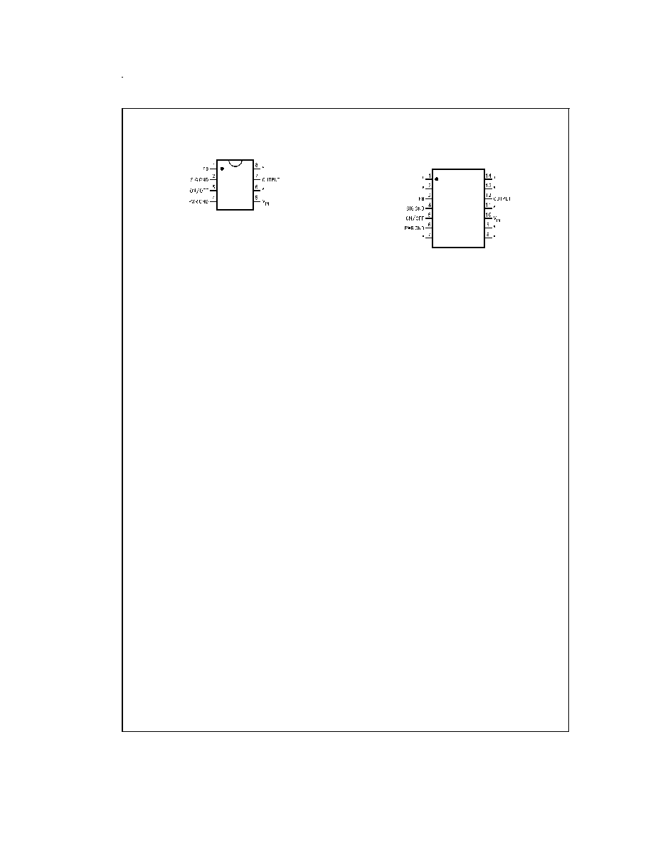
Connection Diagrams
8-Lead DIP
DS011394-2
* No internal connection, but should be soldered to PC board for best heat
transfer.
Top View
Order Number LM2574-3.3HVN, LM2574HVN-5.0,
LM2574HVN-12, LM2574HVN-15, LM2574HVN-ADJ,
LM2574N-3.3, LM2574N-5.0, LM2574N-12,
LM2574N-15 or LM2574N-ADJ
See NS Package Number N08A
14-Lead Wide
Surface Mount (WM)
DS011394-3
Top View
Order Number LM2574HVM-3.3, LM2574HVM-5.0,
LM2574HVM-12, LM2574HVM-15, LM2574HVM-ADJ,
LM2574M-3.3 LM2574M-5.0, LM2574M-12,
LM2574M-15 or LM2574M-ADJ
See NS Package Number M14B
www.national.com
2

Absolute Maximum Ratings
(Note 1)
If Military/Aerospace specified devices are required,
please contact the National Semiconductor Sales Office/
Distributors for availability and specifications.
Maximum Supply Voltage
LM2574
45V
LM2574HV
63V
ON /OFF Pin Input Voltage
-0.3V
V
+V
IN
Output Voltage to Ground
(Steady State)
-1V
Minimum ESD Rating
(C = 100 pF, R = 1.5 k
)
2 kV
Storage Temperature Range
-65∞C to +150∞C
Lead Temperature
(Soldering, 10 seconds)
260∞C
Maximum Junction Temperature
150∞C
Power Dissipation
Internally Limited
Operating Ratings
Temperature Range
LM2574/LM2574HV
-40∞C
T
J
+125∞C
Supply Voltage
LM2574
40V
LM2574HV
60V
LM2574-3.3, LM2574HV-3.3
Electrical Characteristics
Specifications with standard type face are for T
J
= 25∞C, and those with boldface type apply over full Operating Tempera-
ture Range.
Symbol
Parameter
Conditions
LM2574-3.3
Units
(Limits)
LM2574HV-3.3
Typ
Limit
(Note 2)
SYSTEM PARAMETERS (Note 3) Test Circuit
Figure 2
V
OUT
Output Voltage
V
IN
= 12V, I
LOAD
= 100 mA
3.3
V
3.234
V(Min)
3.366
V(Max)
V
OUT
Output Voltage
4.75V
V
IN
40V, 0.1A
I
LOAD
0.5A
3.3
V
LM2574
3.168/3.135
V(Min)
3.432/3.465
V(Max)
V
OUT
Output Voltage
4.75V
V
IN
60V, 0.1A
I
LOAD
0.5A
3.3
LM2574HV
3.168/3.135
V(Min)
3.450/3.482
V(Max)
Efficiency
V
IN
= 12V, I
LOAD
= 0.5A
72
%
LM2574-5.0, LM2574HV-5.0
Electrical Characteristics
Specifications with standard type face are for T
J
= 25∞C, and those with boldface type apply over full Operating Tempera-
ture Range.
Symbol
Parameter
Conditions
LM2574-5.0
Units
(Limits)
LM2574HV-5.0
Typ
Limit
(Note 2)
SYSTEM PARAMETERS (Note 3) Test Circuit
Figure 2
V
OUT
Output Voltage
V
IN
= 12V, I
LOAD
= 100 mA
5
V
4.900
V(Min)
5.100
V(Max)
V
OUT
Output Voltage
7V
V
IN
40V, 0.1A
I
LOAD
0.5A
5
V
LM2574
4.800/4.750
V(Min)
5.200/5.250
V(Max)
V
OUT
Output Voltage
7V
V
IN
60V, 0.1A
I
LOAD
0.5A
5
LM2574HV
4.800/4.750
V(Min)
5.225/5.275
V(Max)
Efficiency
V
IN
= 12V, I
LOAD
= 0.5A
77
%
www.national.com
3

LM2574-12, LM2574HV-12
Electrical Characteristics
Specifications with standard type face are for T
J
= 25∞C, and those with boldface type apply over full Operating Tempera-
ture Range.
Symbol
Parameter
Conditions
LM2574-12
Units
(Limits)
LM2574HV-12
Typ
Limit
(Note 2)
SYSTEM PARAMETERS (Note 3) Test Circuit
Figure 2
V
OUT
Output Voltage
V
IN
= 25V, I
LOAD
= 100 mA
12
V
11.76
V(Min)
12.24
V(Max)
V
OUT
Output Voltage
15V
V
IN
40V, 0.1A
I
LOAD
0.5A
12
V
LM2574
11.52/11.40
V(Min)
12.48/12.60
V(Max)
V
OUT
Output Voltage
15V
V
IN
60V, 0.1A
I
LOAD
0.5A
12
LM2574HV
11.52/11.40
V(Min)
12.54/12.66
V(Max)
Efficiency
V
IN
= 15V, I
LOAD
= 0.5A
88
%
LM2574-15, LM2574HV-15
Electrical Characteristics
Specifications with standard type face are for T
J
= 25∞C, and those with boldface type apply over full Operating Tempera-
ture Range.
Symbol
Parameter
Conditions
LM2574-15
Units
(Limits)
LM2574HV-15
Typ
Limit
(Note 2)
SYSTEM PARAMETERS (Note 3) Test Circuit
Figure 2
V
OUT
Output Voltage
V
IN
= 30V, I
LOAD
= 100 mA
15
V
14.70
V(Min)
15.30
V(Max)
V
OUT
Output Voltage
18V
V
IN
40V, 0.1A
I
LOAD
0.5A
15
V
LM2574
14.40/14.25
V(Min)
15.60/15.75
V(Max)
V
OUT
Output Voltage
18V
V
IN
60V, 0.1A
I
LOAD
0.5A
15
LM2574HV
14.40/14.25
V(Min)
15.68/15.83
V(Max)
Efficiency
V
IN
= 18V, I
LOAD
= 0.5A
88
%
LM2574-ADJ, LM2574HV-ADJ
Electrical Characteristics
Specifications with standard type face are for T
J
= 25∞C, and those with boldface type apply over full Operating Tempera-
ture Range. Unless otherwise specified, V
IN
= 12V, I
LOAD
= 100 mA.
Symbol
Parameter
Conditions
LM2574-ADJ
Units
(Limits)
LM2574HV-ADJ
Typ
Limit
(Note 2)
SYSTEM PARAMETERS (Note 3) Test Circuit
Figure 2
V
FB
Feedback Voltage
V
IN
= 12V, I
LOAD
= 100 mA
1.230
V
1.217
V(Min)
1.243
V(Max)
www.national.com
4

LM2574-ADJ, LM2574HV-ADJ
Electrical Characteristics
(Continued)
Specifications with standard type face are for T
J
= 25∞C, and those with boldface type apply over full Operating Tempera-
ture Range. Unless otherwise specified, V
IN
= 12V, I
LOAD
= 100 mA.
Symbol
Parameter
Conditions
LM2574-ADJ
Units
(Limits)
LM2574HV-ADJ
Typ
Limit
(Note 2)
SYSTEM PARAMETERS (Note 3) Test Circuit
Figure 2
V
FB
Feedback Voltage
7V
V
IN
40V, 0.1A
I
LOAD
0.5A
1.230
V
LM2574
V
OUT
Programmed for 5V. Circuit of
Figure 2
1.193/1.180
V(Min)
1.267/1.280
V(Max)
V
FB
Feedback Voltage
7V
V
IN
60V, 0.1A
I
LOAD
0.5A
1.230
LM2574HV
V
OUT
Programmed for 5V. Circuit of
Figure 2
1.193/1.180
V(Min)
1.273/1.286
V(Max)
Efficiency
V
IN
= 12V, V
OUT
= 5V, I
LOAD
= 0.5A
77
%
All Output Voltage Versions
Electrical Characteristics
Specifications with standard type face are for T
J
= 25∞C, and those with boldface type apply over full Operating Tempera-
ture Range. Unless otherwise specified, V
IN
= 12V for the 3.3V, 5V, and Adjustable version, V
IN
= 25V for the 12V version,
and V
IN
= 30V for the 15V version. I
LOAD
= 100 mA.
Symbol
Parameter
Conditions
LM2574-XX
Units
(Limits)
LM2574HV-XX
Typ
Limit
(Note 2)
DEVICE PARAMETERS
I
b
Feedback Bias
Current
Adjustable Version Only, V
OUT
= 5V
50
100/500
nA
f
O
Oscillator Frequency
(see Note 10)
52
kHz
47/42
kHz(Min)
58/63
kHz(Max)
V
SAT
Saturation Voltage
I
OUT
= 0.5A (Note 4)
0.9
V
1.2/1.4
V(max)
DC
Max Duty Cycle
(ON)
(Note 5)
98
%
93
%(Min)
I
CL
Current Limit
Peak Current, (Notes 4, 10)
1.0
A
0.7/0.65
A(Min)
1.6/1.8
A(Max)
I
L
Output Leakage
(Notes 6, 7)
Output = 0V
2
mA(Max)
Current
Output = -1V
7.5
mA
Output = -1V
30
mA(Max)
I
Q
Quiescent Current
(Note 6)
5
mA
10
mA(Max)
I
STBY
Standby Quiescent
ON /OFF Pin= 5V (OFF)
50
µA
Current
200
µA(Max)
JA
Thermal Resistance
N Package, Junction to Ambient (Note 8)
92
JA
N Package, Junction to Ambient (Note 9)
72
∞C/W
JA
M Package, Junction to Ambient (Note 8)
102
JA
M Package, Junction to Ambient (Note 9)
78
www.national.com
5