 | –≠–ª–µ–∫—Ç—Ä–æ–Ω–Ω—ã–π –∫–æ–º–ø–æ–Ω–µ–Ω—Ç: LM26001 | –°–∫–∞—á–∞—Ç—å:  PDF PDF  ZIP ZIP |

LM26001
1.5A Switching Regulator with High Efficiency Sleep
Mode
General Description
The LM26001 is a switching regulator designed for the high
efficiency requirements of applications with stand-by modes.
The device features a low-current sleep mode to maintain
efficiency under light-load conditions and current-mode con-
trol for accurate regulation over a wide input voltage range.
Quiescent current is reduced to 10 µA typically in shutdown
mode and less than 40 µA in sleep mode. Forced PWM
mode is also available to disable sleep mode.
The LM26001 can deliver up to 1.5A of continuous load
current with a fixed current limit, through the internal
N-channel switch. The part has a wide input voltage range of
4.0V to 38V and can operate with input voltages as low as
3V during line transients.
Operating frequency is adjustable from 150 kHz to 500 kHz
with a single resistor and can be synchronized to an external
clock.
Other features include Power good, adjustable soft-start,
enable pin, input under-voltage protection, and an internal
bootstrap diode for reduced component count.
Features
n
High efficiency sleep mode
n
40 µA typical Iq in sleep mode
n
10 µA typical Iq in shutdown mode
n
3.0V minimum input voltage
n
4.0V to 38V continuous input range
n
1.5% reference accuracy
n
Cycle-by-cycle current limit
n
Adjustable Frequency (150 kHz to 500 kHz)
n
Synchronizable to an external clock
n
Power Good Flag
n
Forced PWM function
n
Adjustable Soft-start
n
TSSOP-16 exposed pad package
n
Thermal Shut Down
Applications
n
Automotive Telematics
n
Navigation systems
n
In-Dash Instrumentation
n
Battery Powered Applications
n
Stand-by power for home gateways/set-top boxes
Typical Application Circuit
20179401
PRELIMINARY
May 2006
LM26001
1.5A
Switching
Regulator
with
High
Efficiency
Sleep
Mode
© 2006 National Semiconductor Corporation
DS201794
www.national.com

Connection Diagram
20179402
Top View
16-Lead Plastic TSSOP
Ordering Information
Order Number
Package Type
Package Drawing
Package Marking
Supplied As
LM26001MXA
TSSOP-16EXP
MXA16A
LM26001EM
92 Units of Rail
LM26001MXAX
TSSOP-16EXP
MXA16A
LM26001EM
2500 Units of Tape and Reel
Pin Descriptions
Pin #
Pin Name
Description
1
VIN
Power supply input
2
VIN
Power supply input
3
PGOOD
Power Good pin. An open drain output which goes high when the output voltage is greater than
92% of nominal.
4
EN
Enable is an analog level input pin. When pulled below 0.8V, the device enters shutdown
mode.
5
SS
Soft-start pin. Connect a capacitor from this pin to GND to set the soft-start time.
6
COMP
Compensation pin. Connect to a resistor capacitor pair to compensate the control loop.
7
FB
Feedback pin. Connect to a resistor divider between Vout and GND to set output voltage.
8
GND
Ground
9
FREQ
Frequency adjust pin. Connect a resistor from this pin to GND to set the operating frequency.
10
FPWM
FPWM is a logic level input pin. For normal operation, connect to GND. When pulled high,
sleep mode operation is disabled.
11
SYNC
Frequency synchronization pin. Connect to an external clock signal for synchronized operation.
SYNC must be pulled low for non-synchronized operation.
12
VBIAS
Connect to an external 3V or greater supply to bypass the internal regulator for improved
efficiency. If not used, VBIAS should be tied to GND.
13
VDD
The output of the internal regulator. Bypass with a minimum 1.0 µF capacitor.
14
BOOT
Bootstrap capacitor pin. Connect a 0.1µF minimum ceramic capacitor from this pin to SW to
generate the gate drive bootstrap voltage.
15
SW
Switch pin. The source of the internal N-channel switch.
16
SW
Switch pin. The source of the internal N-channel switch.
EP
EP
Exposed Pad thermal connection. Connect to GND.
LM26001
www.national.com
2

Absolute Maximum Ratings
(Note 1)
If Military/Aerospace specified devices are required,
please contact the National Semiconductor Sales Office/
Distributors for availability and specifications.
Voltages from the indicated pins to GND:
VIN
-0.3V to 40V
SW (Note 7)
-0.5V to 40V
VDD
-0.3V to 7V
VBIAS
-0.3V to 10V
FB
-0.3V to 6V
BOOT
SW-0.3V to SW+7V
PGOOD
-0.3V to 7V
FREQ
-0.3V to 7V
SYNC
-0.3V to 7V
EN
-0.3V to 40V
FPWM
-0.3V to 7V
SS
-0.3V to 7V
Storage Temperature
-65∞C to +150∞C
Power Dissipation (Note 2)
2.6 W
Recommended Lead
Temperature
Vapor Phase (70s)
215∞C
Infrared (15s)
220∞C
ESD Susceptibility (Note 3)
Machine Model
200V
Human Body Model
2KV
Charged Device Model
1kV
Operating Ratings
(Note 1)
Operating Junction Temp.
-40∞C to 125∞C
Supply Voltage (Note 4)
3.0V to 38V
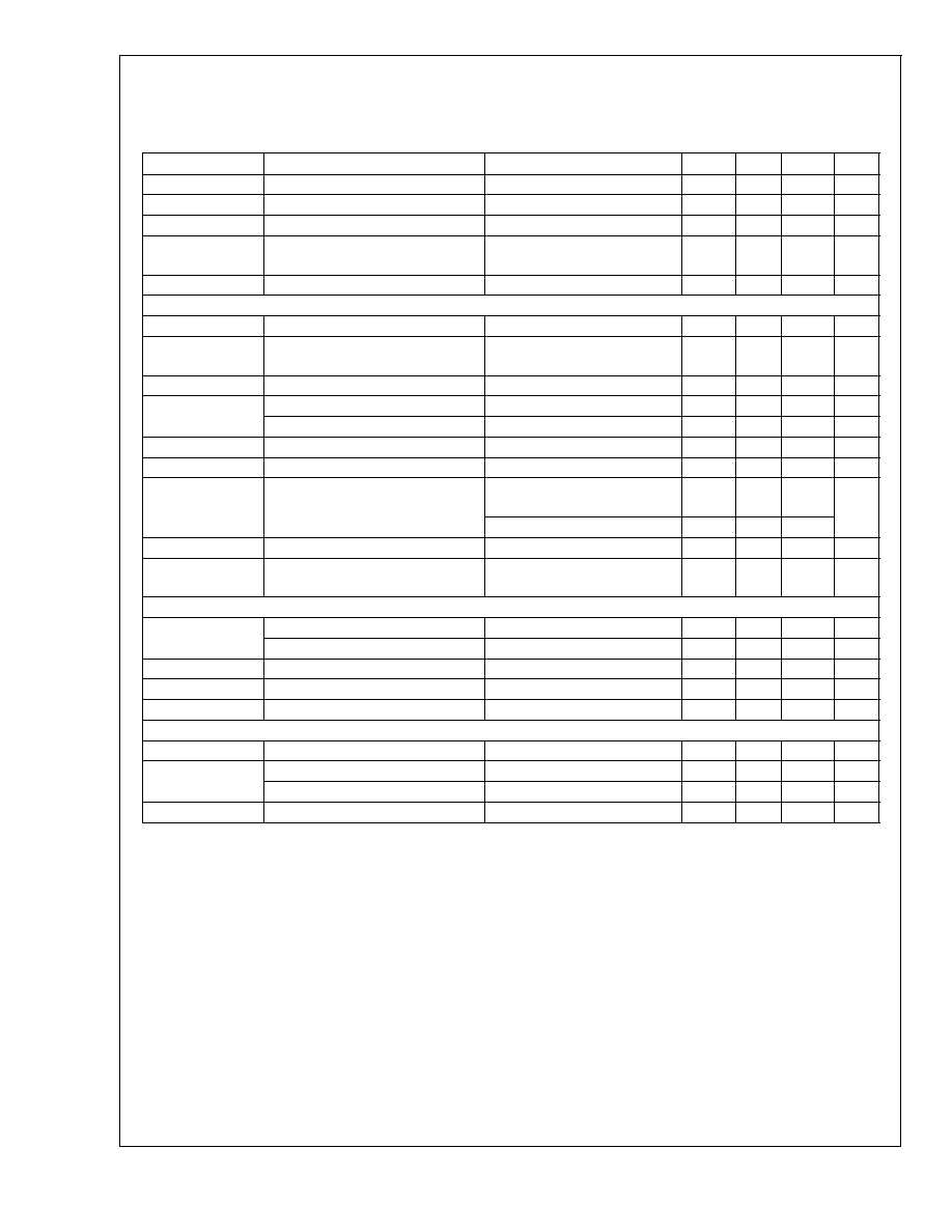
Electrical Characteristics
Specifications in standard type are for T
J
= 25∞C only, and limits in boldface type
apply over the junction temperature (T
J
) range of -40∞C to +125∞C. Unless otherwise stated, Vin=12V. Minimum and Maxi-
mum limits are guaranteed through test, design, or statistical correlation. Typical values represent the most likely parametric
norm at T
J
= 25∞C, and are provided for reference purposes only. (Note 5)
Symbol
Parameter
Conditions
Min
Typ
Max
Unit
System
I
SD
(Note 6)
Shutdown Current
EN = 0V
9.5
20
µA
Iq
_Sleep_VB
(Note
6)
Quiescent Current
Sleep mode, VBIAS = 5V
38
70
µA
Iq
_Sleep_VDD
Quiescent Current
Sleep mode, VBIAS = GND
83
150
µA
Iq
_PWM_VB
Quiescent Current
PWM mode, VBIAS = 5V
150
230
µA
Iq
_PWM_VDD
Quiescent Current
PWM mode, VBIAS = GND
0.65
0.85
mA
I
BIAS_Sleep
(Note 6) Bias Current
Sleep mode, VBIAS = 5V
43
105
µA
I
BIAS_PWM
Bias Current
PWM mode, VBIAS = 5V
0.5
0.70
mA
V
FB
Feedback Voltage
5V
<
Vin
<
38V
1.2155
1.234
1.2525
V
I
FB
FB Bias Current
±
200
nA
V
OUT
/
V
IN
Vout line regulation
5V
<
Vin
<
38V
0.001
%/V
V
OUT
/
I
OUT
Vout load regulation
0.8
<
V
COMP
<
1.15V
0.07
%
VDD
VDD output voltage
7
<
Vin
<
35V, I
VDD
= 0 mA to
5 mA
5.50
5.95
6.50
V
I
SS_Source
Soft-start source current
1.0
2.3
3.5
µA
V
bias_th
VBIAS switchover threshold
2.5
2.7
3.0
V
Switching
R
DS(ON)
Switch on Resistance
Isw = 1A
0.12
0.2
0.40
I
sw_off
Switch off state leakage current
Vin = 38V, VSW = 0V
0.002
5.0
µA
f
sw
Switching Frequency
RFREQ = 62k, 124k, 240k
±
10
%
V
FREQ
FREQ voltage
1.0
V
f
SW
range
Switching Frequency range
150
500
kHz
V
SYNC
Sync pin threshold
SYNC rising
1.2
1.6
V
SYNC falling
0.8
1.1
Sync pin hysteresis
114
mV
I
SYNC
SYNC leakage current
6
nA
F
SYNC_UP
Upper frequency synchronization
range
As compared to nominal f
SW
+30
%
F
SYNC_DN
Lower frequency synchronization
range
As compared to nominal f
SW
-20
%
LM26001
www.national.com
3
Electrical Characteristics
Specifications in standard type are for T
J
= 25∞C only, and limits in boldface type
apply over the junction temperature (T
J
) range of -40∞C to +125∞C. Unless otherwise stated, Vin=12V. Minimum and
Maximum limits are guaranteed through test, design, or statistical correlation. Typical values represent the most likely
parametric norm at T
J
= 25∞C, and are provided for reference purposes only. (Note 5) (Continued)
Symbol
Parameter
Conditions
Min
Typ
Max
Unit
T
OFFMIN
Minimum Off-time
365
ns
T
ONMIN
Minimum On-time
155
ns
TH
SLEEP_HYS
Sleep mode threshold hysteresis
VFB rising, % of TH
WAKE
101.2
%
TH
WAKE
Wake up threshold
Measured at falling FB, COMP
= 0.6V
1.234
V
I
BOOT
BOOT pin leakage current
BOOT = 16V, SW = 10V
0.0006
5.0
µA
Protection
I
LIMPK
Peak Current Limit
1.85
2.5
3.10
A
V
FB_SC
Short circuit frequency foldback
threshold
Measured at FB falling
0.87
V
F_min_sc
Min Frequency in foldback
VFB
<
0.3V
71
kHz
V
TH_PGOOD
Power Good Threshold
Measured at FB, PGOOD rising
89
92
95
%
PGOOD hysteresis
2
7
8
%
I
PGOOD_HI
PGOOD leakage current
PGOOD = 5V
0.2
nA
R
DS_PGOOD
PGOOD on resistance
PGOOD sink current = 500 µA
64
V
UVLO
Under-voltage Lock-Out Threshold
Vin falling , shutdown, VDD =
VIN
2.60
2.9
3.20
V
Vin rising, soft-start, VDD = VIN
3.60
3.9
4.20
TSD
Thermal Shutdown Threshold
160
∞C
JA
Thermal resistance
Power dissipation = 1W, 0 lfpm
air flow
38
∞C/W
Logic
Vth
EN
Enable Threshold voltage
0.8
1.1
1.4
V
Enable hysteresis
164
mV
I
EN_Source
EN source current
EN = 0V
4.5
µA
V
TH_FPWM
FPWM threshold
0.8
1.2
1.6
V
I
FPWM
FPWM leakage current
FPWM = 5V
66
nA
EA
gm
Error amp trans-conductance
400
670
1000
µmho
I
COMP
COMP source current
VCOMP = 0.9V
56
µA
COMP sink current
VCOMP = 0.9V
39
µA
V
COMP
COMP pin voltage range
0.61
1.32
V
Note 1: Absolute Maximum Ratings indicate limits beyond which damage to the device may occur. Operating Ratings indicate conditions for which the device is
intended to be functional, but do not guarantee specific performance limits. For guaranteed specifications and test conditions, see the Electrical Characteristics.
Note 2: The maximum allowable power dissipation is a function of the maximum junction temperature, T
J_MAX
, the junction-to-ambient thermal resistance,
JA
, and
the ambient temperature, T
A
. The maximum allowable power dissipation at any ambient temperature is calculated using: P
D_MAX
= (T
J_MAX
- T
A
) /
JA
. The maximum
power dissipation of 2.6W is determined using T
A
= 25∞C,
JA
= 38∞C/W, and T
J_MAX
= 125∞C.
Note 3: The human body model is a 100 pF capacitor discharged through a 1.5 k
resistor into each pin. The machine model is a 200pF capacitor discharged
directly into each pin. The charged device model is per JESD22-C101-C.
Note 4: Below 4.0V input, power dissipation may increase due to increased R
DS(ON)
. Therefore, a minimum input voltage of 4.0V is required to operate continuously
within specification. A minimum of 3.9V (typical) is also required for startup.
Note 5: All room temperature limits are 100% production tested. All limits at temperature extremes are guaranteed through correlation using standard Statistical
Quality Control (SQC) methods. All limits are used to calculate Average Outgoing Quality Level (AOQL).
Note 6: Iq and ISD specify the current into the VIN pin. IBIAS is the current into the VBIAS pin when the VBIAS voltage is greater than 3V. All quiescent current
specifications apply to non-switching operation.
Note 7: The absolute maximum specification applies to DC voltage. An extended negative voltage limit of -2V applies for a pulse of up to 1µs, and -1V for a pulse
of up to 20µs.
LM26001
www.national.com
4

Typical Performance Characteristics
Unless otherwise specified the following conditions apply: Vin
= 12V, T
J
= 25∞C.
VFB vs Temperature
VFB vs Vin
(IDC = 300 mA)
20179403
20179405
IQ and IVBIAS vs Temperature (Sleep Mode)
IQ and IVBIAS vs Temperature (PWM Mode)
20179404
20179406
Normalized Switching Frequency vs Temperature
(300kHz)
UVLO Threshold vs Temperature (VDD= VIN)
20179416
20179417
LM26001
www.national.com
5