LM2611
1.4MHz Cuk Converter
General Description
The LM2611 is a current mode, PWM inverting switching
regulator. Operating from a 2.7 - 14V supply, it is capable of
producing a regulated negative output voltage of up to
-(36-V
IN(MAX)
). The LM2611 utilizes an input and output
inductor, which enables low voltage ripple and RMS current
on both the input and the output. With a switching frequency
of 1.4MHz, the inductors and output capacitor can be physi-
cally small and low cost. High efficiency is achieved through
the use of a low R
DS(ON)
FET.
The LM2611 features a shutdown pin, which can be acti-
vated when the part is not needed to lower the Iq and save
battery life. A negative feedback (NFB) pin provides a simple
method of setting the output voltage, using just two resistors.
Cycle-by-cycle current limiting and internal compensation
further simplify the use of the LM2611.
The LM2611 is available is a small SOT23-5 package. It
comes in two grades:
Grade A
Grade B
Current Limit
1.2A
0.9A
R
DS(ON)
0.5
0.7
Features
n
1.4MHz switching frequency
n
Low R
DS(ON)
DMOS FET
n
1mVp-p output ripple
n
-5V at 300mA from 5V input
n
Better regulation than a charge pump
n
Uses tiny capacitors and inductors
n
Wide input range: 2.7V to 14V
n
Low shutdown current:
<
1uA
n
5-lead SOT-23 package
Applications
n
MR Head Bias
n
Digital camera CCD bias
n
LCD bias
n
GaAs FET bias
n
Positive to negative conversion
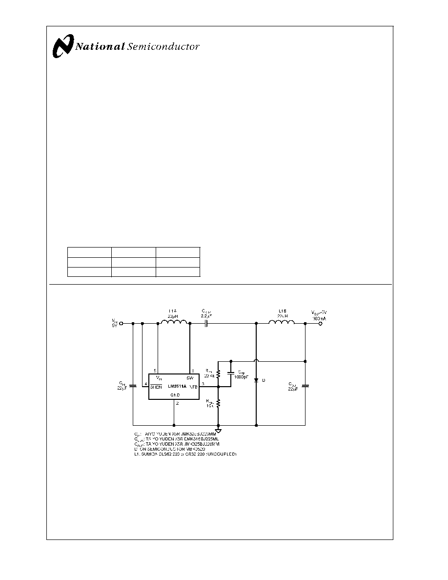
Typical Application Circuit
20018117
January 2002
LM261
1
1.4MHz
Cuk
Converter
� 2002 National Semiconductor Corporation
DS200181
www.national.com
Connection Diagram
Top View
20018115
5-lead SOT-23 Package
NS Package Number MF05A
Ordering Information
Order Number
Package Type
NSC Package
Drawing
Supplied As
Package ID
LM2611AMF
SOT23-5
MF05A
1K Tape and Reel
S40A
LM2611AMFX
3K Tape and Reel
S40A
LM2611BMF
1K Tape and Reel
S40B
LM2611BMFX
3K Tape and Reel
S40B
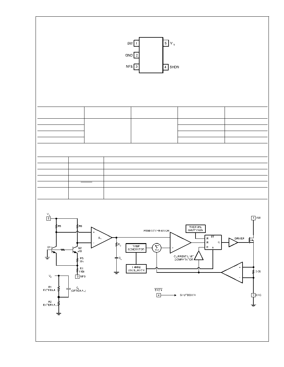
Pin Description
Pin
Name
Function
1
SW
Drain of internal switch. Connect at the node of the input inductor and Cuk capacitor.
2
GND
Analog and power ground.
3
NFB
Negative feedback. Connect to output via external resistor divider to set output voltage.
4
SHDN
Shutdown control input. V
IN
= Device on. Ground = Device in shutdown.
5
V
IN
Analog and power input. Filter out high frequency noise with a 0.1 �F ceramic capacitor
placed close to the pin.
Block Diagram
20018101
LM261
1
www.national.com
2
Absolute Maximum Ratings
(Note 1)
If Military/Aerospace specified devices are required,
please contact the National Semiconductor Sales Office/
Distributors for availability and specifications.
V
IN
14.5V
SW Voltage
-0. 4V to 36V
NFB Voltage
+0. 4V to -6V
SHDN Voltage
-0. 4V to 14.5V
Maximum Junction
Temperature
125�C
Power Dissipation (Note 2)
Internally Limited
Lead Temperature
300�C
ESD Susceptibility (Note 3)
Human Body Model
2kV
Machine Model
200V
Operating Conditions
Operating Junction
Temperature Range
(Note 4)
-40�C to +125�C
Storage Temperature
-65�C to +150�C
Supply Voltage
2.7V to 14V
JA
256�C/W
Electrical Characteristics
Specifications in standard type face are for T
J
= 25�C and those with boldface type apply over the full Operating Tempera-
ture Range ( T
J
= -40�C to +85�C) unless otherwise specified. V
IN
= 5.0V and I
L
= 0A, unless otherwise specified.
Symbol
Parameter
Conditions
Min
(Note 4)
Typ
(Note 5)
Max
(Note 4)
Units
V
IN
Input Voltage
2.7
14
V
I
SW
Switch Current Limit
Grade A
1
1.2
2
A
Grade B
0.7
0.9
R
DSON
Switch ON Resistance
Grade A
0.5
0.65
Grade B
0.7
0.9
SHDN
TH
Shutdown Threshold
Device enabled
1.5
V
Device disabled
0.50
I
SHDN
Shutdown Pin Bias Current
V
SHDN
= 0V
0.0
�A
V
SHDN
= 5V
0.0
1.0
NFB
Negative Feedback
Reference
V
IN
= 3V
-1.205
-1.23
-1.255
V
I
NFB
NFB Pin Bias Current
V
NFB
=-1.23V
-2.7
-4.7
-6.7
�A
I
q
Quiescent Current
V
SHDN
= 5V, Switching
1.8
3.5
mA
V
SHDN
= 5V, Not Switching
270
500
�A
V
SHDN
= 0V
0.024
1
�A
%V
OUT
/
V
IN
Reference Line Regulation
2.7V
V
IN
14V
0.02
%/V
f
S
Switching Frequency
1.0
1.4
1.8
MHz
D
MAX
Maximum Duty Cycle
82
88
%
I
L
Switch Leakage
Not Switching
V
SW
= 5V
1
�A
Note 1: Absolute maximum ratings are limits beyond which damage to the device may occur. Operating Ratings are conditions for which the device is intended to
be functional, but device parameter specifications may not be guaranteed. For guaranteed specifications and test conditions, see the Electrical Characteristics.
Note 2: The maximum allowable power dissipation is a function of the maximum junction temperature, T
J
(MAX), the junction-to-ambient thermal resistance,
JA
,
and the ambient temperature, T
A
. See the Electrical Characteristics table for the thermal resistance of various layouts. The maximum allowable power dissipation
at any ambient temperature is calculated using: P
D
(MAX) = (T
J(MAX)
- T
A
)/
JA
. Exceeding the maximum allowable power dissipation will cause excessive die
temperature, and the regulator will go into thermal shutdown.
Note 3: The human body model is a 100 pF capacitor discharged through a 1.5k
resistor into each pin. The machine model is a 200pF capacitor discharged
directly into each pin.
Note 4: All limits guaranteed at room temperature (standard typeface) and at temperature extremes (bold typeface). All room temperature limits are 100% tested
or guaranteed through statistical analysis. All limits at temperature extremes are guaranteed via correlation using standard Statistical Quality Control (SQC) methods.
All limits are used to calculate Average Outgoing Quality Level (AOQL).
Note 5: Typical numbers are at 25�C and represent the expected value of the parameter.
LM261
1
www.national.com
3
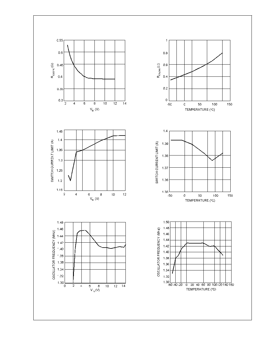
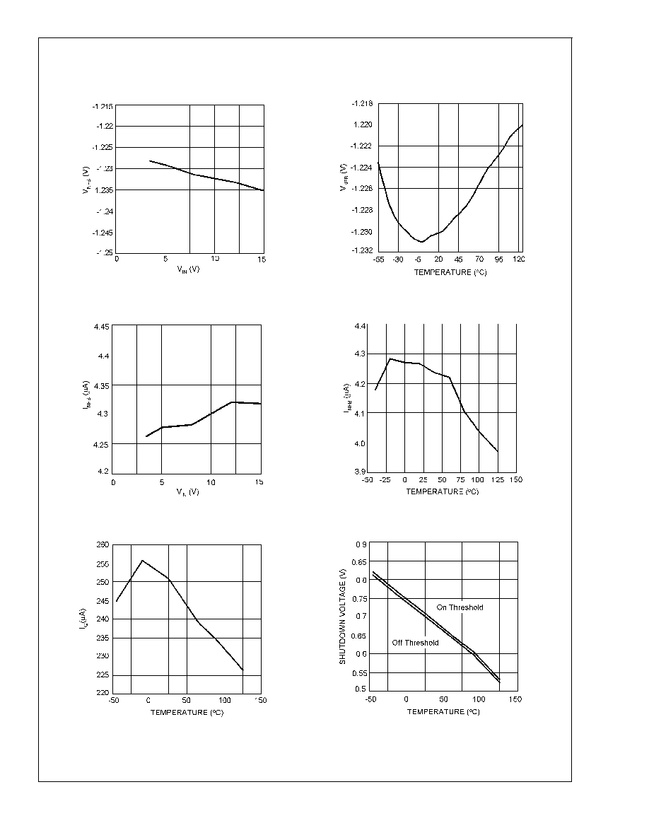
Typical Performance Characteristics
R
DS(ON)
vs V
IN
R
DS(ON)
Vs. Ambient Temperature
V
IN
= 5V
20018112
20018145
Switch Current Limit vs. V
IN
Switch Current Limit vs Ambient Temperature
V
IN
= 5V
20018111
20018143
Oscillator Frequency vs V
IN
Oscillator Frequency vs Ambient Temperature
V
IN
= 5V
20018119
20018116
LM261
1
www.national.com
4