 | –≠–ª–µ–∫—Ç—Ä–æ–Ω–Ω—ã–π –∫–æ–º–ø–æ–Ω–µ–Ω—Ç: LM2621MM | –°–∫–∞—á–∞—Ç—å:  PDF PDF  ZIP ZIP |

LM2621
Low Input Voltage, Step-Up DC-DC Converter
General Description
The LM2621 is a high efficiency, step-up DC-DC switching
regulator for battery-powered and low input voltage systems.
It accepts an input voltage between 1.2V and 14V and con-
verts it into a regulated output voltage. The output voltage
can be adjusted between 1.24V and 14V. It has an internal
0.17
N-Channel MOSFET power switch. Efficiencies up to
90% are achievable using the LM2621.
The high switching frequency (adjustable up to 2MHz) of the
LM2621 allows for tiny surface mount inductors and capaci-
tors. Because of the unique constant-duty-cycle gated oscil-
lator topology very high efficiencies are realized over a wide
load range. The supply current is reduced to 80µA because
of the BiCMOS process technology. In the shutdown mode,
the supply current is less than 2.5µA.
The LM2621 is available in a Mini-SO-8 package. This pack-
age uses half the board area of a standard 8-pin SO and has
a height of just 1.09 mm.
Features
n
Small Mini-SO8 Package (Half the Footprint of Standard
8-Pin SO Package)
n
1.09 mm Package Height
n
Up to 2 MHz Switching Frequency
n
1.2V to 14V Input Voltage
n
1.24V - 14V Adjustable Output Voltage
n
Up to 1A Load Current
n
0.17
Internal MOSFET
n
Up to 90% Regulator Efficiency
n
80 µA Typical Operating Current
n
<
2.5µA Guaranteed Supply Current In Shutdown
Applications
n
PDAs, Cellular Phones
n
2-Cell and 3-Cell Battery-Operated Equipment
n
PCMCIA Cards, Memory Cards
n
Flash Memory Programming
n
TFT/LCD Applications
n
3.3V to 5.0V Conversion
n
GPS Devices
n
Two-Way Pagers
n
Palmtop Computers
n
Hand-Held Instruments
Typical Application Circuit
DS100934-12
February 2000
LM2621
Low
Input
V
oltage,
Step-Up
DC-DC
Converter
© 2000 National Semiconductor Corporation
DS100934
www.national.com

Connection Diagram
Ordering Information
Order Number
Package Type
NSC Package
Drawing
Package
Marking
Supplied As
LM2621MMX
Mini SO-8
MUA08A
S06A
3000 Units on Tape and Reel
LM2621MM
Mini SO-8
MUA08A
S06A
1000 Units on Tape and Reel
Mini SO-8 (MM) Package
DS100934-18
Top View
LM2621
www.national.com
2

Absolute Maximum Ratings
(Note 1)
If Military/Aerospace specified devices are required,
please contact the National Semiconductor Sales Office/
Distributors for availability and specifications.
SW Pin Voltage
-0.5 V to 14.5V
BOOT, V
DD
, EN and FB Pins
-0.5V to 10V
FREQ Pin
100µA
JA
(Note 2)
240∞C/W
T
Jmax
(Note 2)
150∞C
Storage Temperature Range
-65∞C to +150∞C
Lead Temp. (Soldering, 5 sec)
260∞C
Power Dissipation (T
A
=25∞C)
(Note 2)
500mW
ESD Rating (Note 3)
2kV
Operating Conditions
(Note 1)
V
DD
Pin
2.5V to 5V
FB, EN Pins
0 to V
DD
BOOT Pin
0 to 10V
Ambient Temperature (T
A
)
-40∞C to +85∞C
Electrical Characteristics
Limits in standard typeface are for T
J
= 25∞C, and limits in boldface type apply over the full operating temperature range of
-40∞C to +85∞C. Unless otherwise specified: V
DD
= V
OUT
= 3.3V.
Symbol
Parameter
Condition
Typ
Min
Max
Units
V
IN_ST
Minimum Start-Up Supply
Voltage (Note 4)
I
LOAD
= 0mA
1.1
1.2
V
V
IN_OP
Minimum Operating Supply
Voltage (once started)
I
LOAD
= 0mA
0.65
V
V
FB
FB Pin Voltage
1.24
1.2028
1.2772
V
V
OUT_MAX
Maximum Output Voltage
14
V
V
HYST
Hysteresis Voltage (Note 7)
30
45
mV
Efficiency
V
IN
= 3.6V; V
OUT
= 5V; I
LOAD
= 500mA
87
%
V
IN
= 2.5V; V
OUT
= 3.3V; I
LOAD
= 200mA
87
D
Switch Duty Cycle
70
60
80
%
I
DD
Operating Quiescent Current
(Note 6)
FB Pin
>
1.3V; EN Pin at V
DD
80
110
µA
I
SD
Shutdown Quiescent Current
(Note 7)
V
DD
, BOOT and SW Pins at
5.0V; EN Pin
<
200mV
0.01
2.5
µA
I
CL
Switch Peak Current Limit
2.85
A
R
DS_ON
MOSFET Switch On
Resistance
0.17
Enable Section
V
EN_LO
EN Pin Voltage Low (Note 8)
0.15V
DD
V
V
EN_HI
EN Pin Voltage High (Note 8)
0.7V
DD
V
Note 1: Absolute maximum ratings indicate limits beyond which damage to the device may occur. Electrical specifications do not apply when operating the device
outside of its rated operating conditions.
Note 2: The maximum power dissipation must be derated at elevated temperatures and is dictated by T
jmax
(maximum junction temperature),
JA
(junction to am-
bient thermal resistance), and T
A
(ambient temperature). The maximum allowable power dissipation at any temperature is P
dmax
= (T
jmax
- T
A
)/
JA
or the number
given in the Absolute Maximum Ratings, whichever is lower.
Note 3: The human body model is a 100 pF capacitor discharged through a 1.5 k
resistor into each pin. For Pin 8 (SW) the ESD rating is 1.5 kV.
Note 4: Output in regulation, V
OUT
= V
OUT (NOMINAL
)
±
5%
Note 5: This is the hysteresis value of the internal comparator used for the gated-oscillator control scheme.
Note 6: This is the current into the V
DD
pin.
Note 7: This is the total current into pins V
DD
, BOOT, SW and FREQ.
Note 8: When the EN pin is below V
EN_LO
, the regulator is shut down; when it is above V
EN_HI
, the regulator is operating.
LM2621
www.national.com
3
Pin Description
Pin
Name
Function
1
PGND
Power Ground
2
EN
Active-Low Shutdown Input
3
FREQ
Frequency Adjust. An external resistor connected between this pin and Pin 6 (V
DD
) sets the
switching frequency of the LM2621.
4
FB
Output Voltage Feedback
5
SGND
Signal Ground
6
V
DD
Power Supply for Internal Circuitry
7
BOOT
Bootstrap Supply for the Gate Drive of Internal MOSFET Power Switch
8
SW
Drain of the Internal MOSFET Power Switch
Typical Performance Characteristics
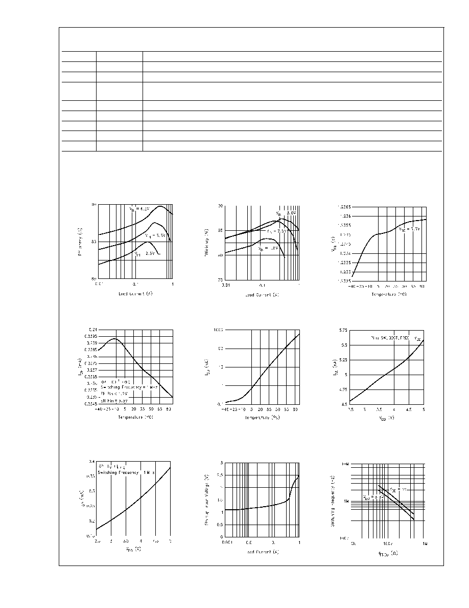
Efficiency vs Load Current
V
OUT
= 5.0V
DS100934-1
Efficiency vs Load Current
V
OUT
= 3.3V
DS100934-2
V
FB
vs Temperature
DS100934-3
I
OP
vs Temperature
DS100934-4
I
SD
vs Temperature
DS100934-5
I
SD
vs V
DD
DS100934-6
I
OP
vs V
DD
DS100934-7
V
IN_ST
vs Load Current
V
OUT
= 3.3V
DS100934-8
Switching Frequency vs R
FQ
DS100934-9
LM2621
www.national.com
4

Typical Performance Characteristics
(Continued)
Detailed Description
OPERATING PRINCIPLE
The LM2621 is designed to provide step-up DC-DC voltage
regulation in battery-powered and low-input voltage sys-
tems. It combines a step-up switching regulator, N-channel
power MOSFET, built-in current limit, thermal limit, and volt-
age reference in a single 8-pin MSOP package . The switch-
ing DC-DC regulator boosts an input voltage between 1.2V
and 14V to a regulated output voltage between 1.24V and
14V. The LM2621 starts from a low 1.1V input and remains
operational down to 0.65V.
This device is optimized for use in cellular phones and other
applications requiring a small size, low profile, as well as low
quiescent current for maximum battery life during stand-by
and shutdown. A high-efficiency gated-oscillator topology of-
fers an output of up to 1A.
Additional features include a built-in peak switch current
limit, and thermal protection circuitry.
GATED OSCILLATOR CONTROL SCHEME
A unique gated oscillator control scheme enables the
LM2621 to have an ultra-low quiescent current and provides
a high efficiency over a wide load range. The switching fre-
quency of the internal oscillator is programmable using an
external resistor and can be set between 300 kHz and 2
MHz.
Peak Inductor Current vs
Load Current
DS100934-10
Maximum Load Current vs
Input Voltage
DS100934-11
DS100934-14
FIGURE 1. Functional Diagram
LM2621
www.national.com
5