 | –≠–ª–µ–∫—Ç—Ä–æ–Ω–Ω—ã–π –∫–æ–º–ø–æ–Ω–µ–Ω—Ç: LM2623LDX | –°–∫–∞—á–∞—Ç—å:  PDF PDF  ZIP ZIP |
LM2623
General Purpose, Gated Oscillator Based, DC/DC Boost
Converter
General Description
The LM2623 is a high efficiency, general purpose, step-up
DC-DC switching regulator for battery-powered and low in-
put voltage systems. It accepts an input voltage between .8
and 14 volts and converts it into a regulated output voltage
between 1.24 and 14 volts. Efficiencies up to 90% are
achievable with the LM2623.
In order to adapt to a number of applications, the LM2623
allows the designer to vary the output voltage, the operating
frequency (300kHz to 2 MHz) and duty cycle (17% to 90%)
to optimize the part's performance. The selected values can
be fixed or can vary with battery voltage or input to output
voltage ratio. The LM2623 uses a very simple, on/off regu-
lation mode to produce good efficiency and stable operation
over a wide operating range. It normally regulates by skip-
ping switching cycles when it reaches the regulation limit
(Pulse Frequency Modulation).
Note: Please read the "Non-Linear Effect" and "Choosing
The Correct C3 Capacitor" sub-sections of the Design Pro-
cedure section of this data sheet, so that any challenges with
designing with this part can be taken into account before a
board design/layout is finalized.
For Alternative Solutions, See Also: LM2700, LM2622,
LM2731, LM2733, and LM2621.
Features
n
Good Efficiency Over a Very Wide Load Range
n
Very Low Output Voltage Ripple
n
Small, Mini-SO-8 Package (Half the Footprint of
Standard 8 pin SO Package)
n
1.09 mm Package Height
n
Up to 2 MHz Switching Frequency
n
.8V to 14V Operating Voltage
n
1.1V Start-up Voltage
n
1.24V - 14V Adjustable Output Voltage
n
Up to 2A Load Current at low Output Voltages
n
0.17
Internal MOSFET
n
Up to 90% Regulator Efficiency
n
80 µA Typical Operating Current (into V
DD
pin of supply)
n
<
2.5µA Guaranteed Supply Current In Shutdown
n
4mm x 4mm Thermally Enhanced LLP Package Option
Applications
n
Cameras, Pagers and Cell Phones
n
PDAs,Palmtop Computers, GPS devices
n
White LED Drive, TFT or Scanned LCDs
n
Flash Memory Programming
n
Hand-Held Instruments
n
1, 2, 3 or 4 Cell Alkaline Systems
n
1, 2 or 3 Cell Lithium-ion Systems
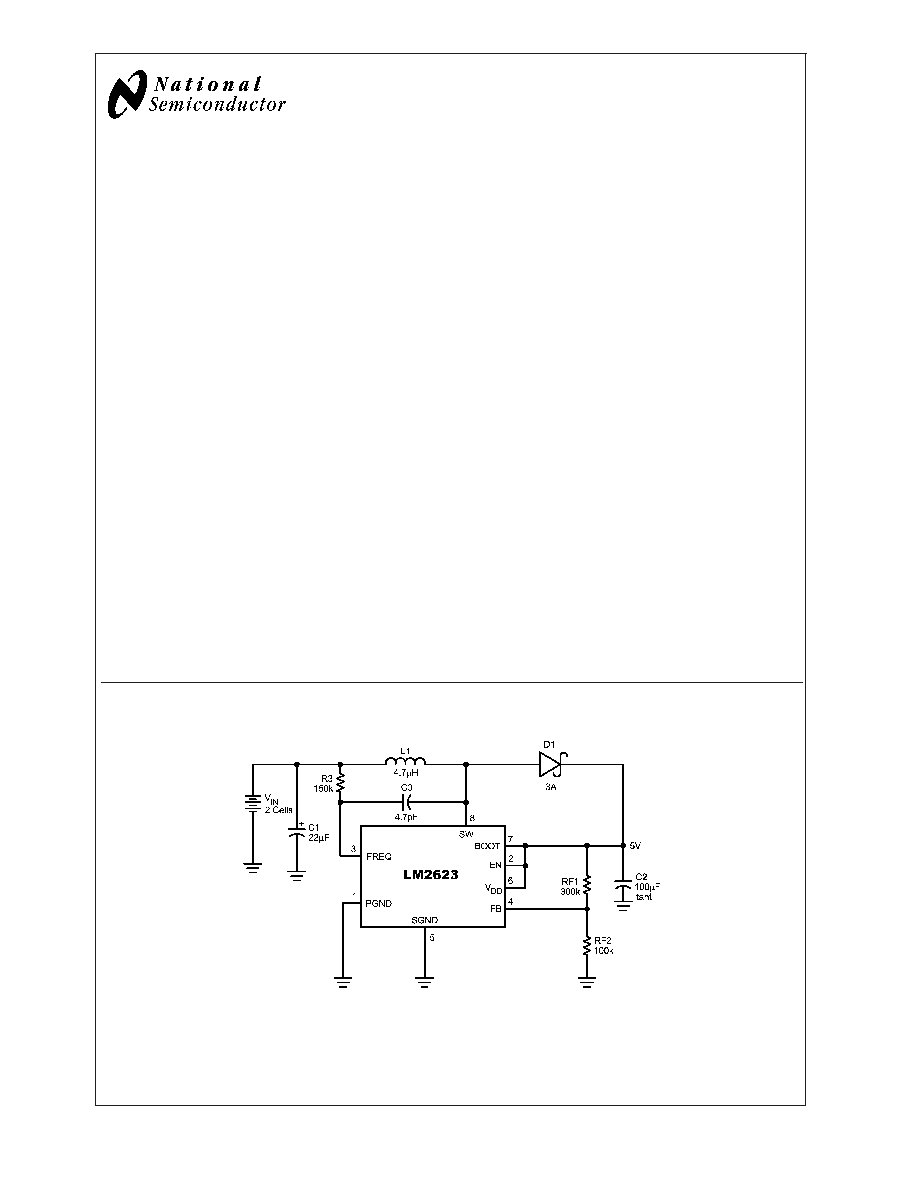
Typical Application Circuit
20038801
July 2003
LM2623
General
Purpose,
Gated
Oscillator
Based,
DC/DC
Boost
Converter
© 2003 National Semiconductor Corporation
DS200388
www.national.com
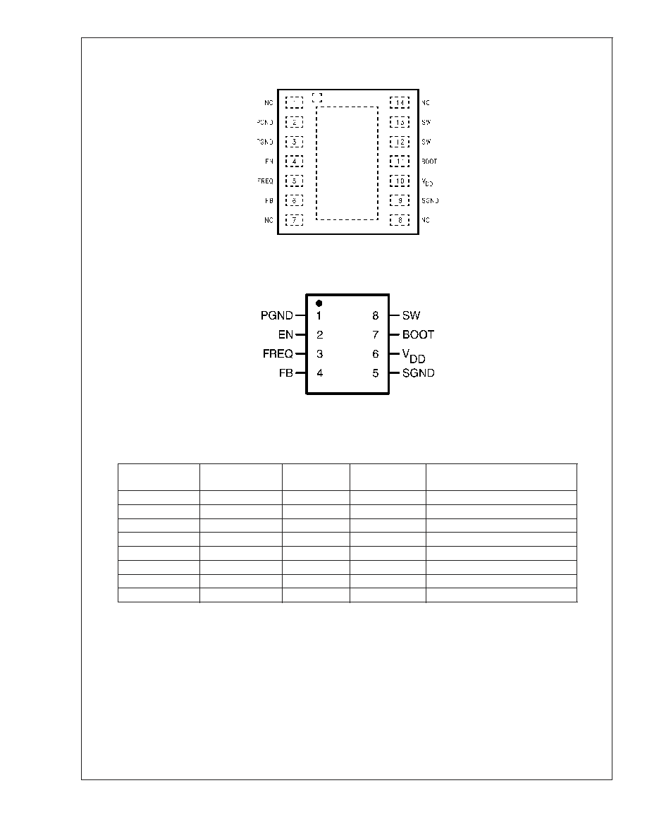
Connection Diagram
LLP Package
20038802
Top View
Mini SO-8 (MM) Package
20038818
Top View
Ordering Information
Order Number
Package Type
NSC Package
Drawing
Package
Marking
Supplied As
LM2623MMX
Mini SO-8
MUA08A
S46B
3000 Units on Tape and Reel
LM2623AMMX
Mini SO-8
MUA08A
S46A
3000 Units on Tape and Reel
LM2623AMM
Mini SO-8
MUA08A
S46A
1000 Units on Tape and Reel
LM2623MM
Mini SO-8
MUA08A
S46B
1000 Units on Tape and Reel
LM2623LDX
LLP-14
LDA14A
2623AB
4500 Units on Tape and Reel
LM2623ALDX
LLP-14
LDA14A
2623A
4500 Units on Tape and Reel
LM2623LD
LLP-14
LDA14A
2623AB
1000 Units on Tape and Reel
LM2623ALD
LLP-14
LDA14A
2623A
1000 Units on Tape and Reel
LM2623
www.national.com
2
Pin Description
LLP-14 Pin
MSOP-8 Pin
Name
Function
1
NC
No Connect
2, 3
1
PGND
Power Ground (LLP Pins 2 & 3 must be shorted
together).
4
2
EN
Active-Low Shutdown Input
5
3
FREQ
Frequency Adjust. An external resistor connected
between this pin and a voltage source sets the
switching frequency of the LM2623.
6
4
FB
Output Voltage Feedback
7
NC
No Connect
8
NC
No connect
9
5
SGND
Signal Ground
10
6
V
DD
Power Supply for Internal Circuitry
11
7
BOOT
Bootstrap Supply for the Gate Drive of Internal
MOSFET Power Switch
12, 13
8
SW
Drain of the Internal MOSFET Power Switch. (LLP Pins
12 & 13 must be shorted together).
14
NC
No Connect
DAP
DAP
To be soldered to board for enhanced thermal
dissipation. To be electrically isolated/floating.
LM2623
www.national.com
3
Absolute Maximum Ratings
(Note 1)
If Military/Aerospace specified devices are required,
please contact the National Semiconductor Sales Office/
Distributors for availability and specifications.
SW Pin Voltage
-0.5 V to 14.5V
BOOT, V
DD
, EN and FB Pins
-0.5V to 10V
FREQ Pin
100µA
T
Jmax
(Note 2)
150∞C
Storage Temperature Range
-65∞C to +150∞C
Lead Temp. (Soldering, 5 sec)
260∞C
Power Dissipation (T
A
=25∞C)
(Note 2)
500mW
ESD Rating (Note 3)
2kV
Operating Conditions
(Note 1)
V
DD
Pin
3V to 5V
FB, EN Pins
0 to V
DD
BOOT Pin
0 to 10V
Ambient Temperature (T
A
)
-40∞C to +85∞C
Electrical Characteristics
Limits in standard typeface are for T
J
= 25∞C, and limits in boldface type apply over the full operating temperature range of
-40∞C to +85∞C. Unless otherwise specified: V
DD
= V
OUT
= 3.3V.
Symbol
Parameter
Condition
Typ
Min
Max
Units
V
DD_ST
Start-Up Supply Voltage 25∞C
I
LOAD
= 0mA (Note 4)
1.1
V
V
IN_OP
Minimum Operating Supply
Voltage (once started)
I
LOAD
= 0mA
0.65
.8
V
V
FB
FB Pin Voltage
1.24
1.2028
1.2772
V
V
OUT_MAX
Maximum Output Voltage
14
V
Efficiency
V
IN
= 3.6V; V
OUT
= 5V; I
LOAD
=
500mA
87
%
V
IN
= 2.5V; V
OUT
= 3.3V; I
LOAD
= 200mA
87
D
Switch Duty Cycle
17
%
I
DD
Operating Quiescent Current
(Note 5)
FB Pin
>
1.3V; EN Pin at V
DD
80
110
µA
I
SD
Shutdown Quiescent Current
(Note 6)
V
DD
, BOOT and SW Pins at
5.0V; EN Pin
<
200mV
0.01
2.5
µA
I
CL
Switch Peak Current Limit
LM2623A
2. 85
2.2
A
I
C
Switch Peak Current Limit
LM2623
1.2
A
R
DS_ON
MOSFET Switch On
Resistance
0.17
0.26
JA
Thermal Resistance
MM Package, Junction to
Ambient(Note 2)
240
∞C/W
JA
Thermal Resistance
LLP Package, Junction to
Ambient(Notes 2, 8)
40
∞C/W
JA
Thermal Resistance
LLP Package, Junction to
Ambient(Notes 2, 9)
56
∞C/W
Enable Section
V
EN_LO
EN Pin Voltage Low (Note 7)
0.15V
DD
V
V
EN_HI
EN Pin Voltage High (Note 7)
0.7V
DD
V
Note 1: Absolute maximum ratings indicate limits beyond which damage to the device may occur. Electrical specifications do not apply when operating the device
outside of its rated operating conditions.
Note 2: The maximum power dissipation must be derated at elevated temperatures and is dictated by T
jmax
(maximum junction temperature),
JA
(junction to
ambient thermal resistance), and T
A
(ambient temperature). The maximum allowable power dissipation at any temperature is P
dmax
= (T
jmax
- T
A
)/
JA
or the number
given in the Absolute Maximum Ratings, whichever is lower.
Note 3: The human body model is a 100 pF capacitor discharged through a 1.5 k
resistor into each pin. For Pin 8 (SW) the ESD rating is 1.0 kV.
Note 4: V
DD
tied to Boot and EN pins. Frequency pin tied to V
DD
through 121K resistor. V
DD_ST
= V
DD
when startu-up occurs. V
IN
is V
DD
+ D1 voltage (usually
10-50 mv at start-up)
Note 5: This is the current into the V
DD
pin.
Note 6: This is the total current into pins V
DD
, BOOT, SW and FREQ.
Note 7: When the EN pin is below V
EN_LO
, the regulator is shut down; when it is above V
EN_HI
, the regulator is operating.
LM2623
www.national.com
4

Electrical Characteristics
(Continued)
Note 8: Junction to ambient thermal resistance (
JA
) is taken from a thermal modeling result, performed under the conditions and guidelines set forthe in the JEDEC
standard JESD51-17. The test board is a 4 layer FR-4 board measuring 102mm x 76mm x 1.6mm with a 3 x 2 array of thermal vias. The ground plane on the board
is 50mm x 50 mm. Thickness of copper layers are 36mm/18mm/18mm/36mm (1.5oz/10z/1oz/1.5ox). Ambient temperature in simulation is 22∞C, still air. Power
dissipation is 1W. (The DAP is soldered.) Fore more information on LLP thermal topics, as well as LLP mounting and soldering specifications please refer to
Application Note 1187: Leadless Leadframe Package (LLP).
Note 9: Exposed DAP soldered to an exposed 1sq. inch area of 1 oz. copper. Thermal resistance can be decreased by using more copper are to dissipate heat.
LM2623
www.national.com
5

Typical Performance Characteristics
Efficiency vs V
IN
V
OUT
= 5.0V
V
FB
vs Temperature
20038829
20038831
Frequency vs V
IN
Maximum Start Up Voltage vs
Temperature
20038828
20038826
Typical R
DS(ON)
vs
Temperature
Typical Current Limit vs
Temperature
20038825
20038827
LM2623
www.national.com
6
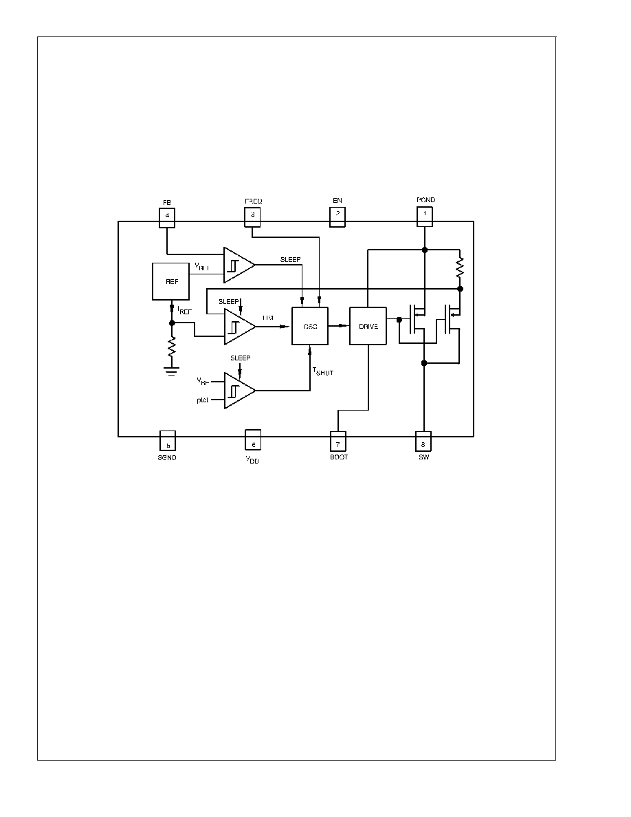
Detailed Description
OPERATING PRINCIPLE
The LM2623 is designed to provide step-up DC-DC voltage
regulation in battery-powered and low-input voltage sys-
tems. It combines a step-up switching regulator, N-channel
power MOSFET, built-in current limit, thermal limit, and volt-
age reference in a single 8-pin MSOP package Figure 1. The
switching DC-DC regulator boosts an input voltage between
.8V and 14V to a regulated output voltage between 1.24V
and 14V. The LM2623 starts from a low 1.1V input and
remains operational down to below .8V.
This device is optimized for use in cellular phones and other
applications requiring a small size, low profile, as well as low
quiescent current for maximum battery life during stand-by
and shutdown. A high-efficiency gated-oscillator topology
offers an output of up to 2A at low output voltages.
Additional features include a built-in peak switch current
limit, and thermal protection circuitry.
GATED OSCILLATOR CONTROL SCHEME
The on/off regulation mode of the LM2623, along with its
ultra-low quiescent current, results in good efficiency over a
very wide load range. The internal oscillator frequency can
be programmed using an external resistor to be constant or
vary with the battery voltage. Adding a capacitor to program
the frequency allows the designer to adjust the duty cycle
and optimize it for the application. Adding a resistor in addi-
tion to the capacitor allows the duty cycle to dynamically
compensate for changes to the input/output voltage ratio.
We call this a Ratio Adaptive Gated Oscillator circuit. See the
Application Notes for sample application circuits. Using the
correct RC components to adjust the oscillator allows the
part to run with low ripple and high efficiency over a wide
range of loads and input/output voltages.
20038814
FIGURE 1. Functional Diagram
LM2623
www.national.com
7
Detailed Description
(Continued)
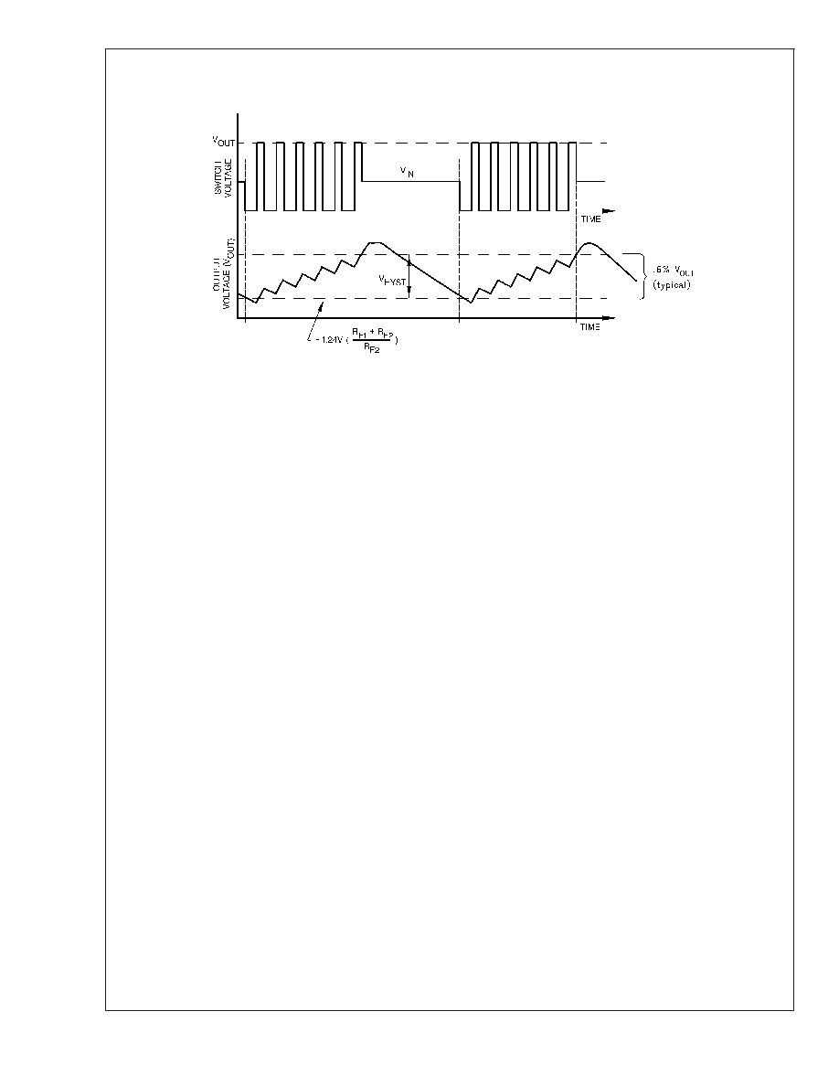
PULSE FREQUENCY MODULATION (PFM)
Pulse Frequency Modulation is typically accomplished by
switching continuously until the voltage limit is reached and
skipping cycles after that to just maintain it. This results in a
somewhat hysteretic mode of operation. The coil stores
more energy each cycle as the current ramps up to high
levels. When the voltage limit is reached, the system usually
overshoots to a higher voltage than required, due to the
stored energy in the coil (see figure 2). The system will also
undershoot somewhat when it starts switching again be-
cause it has depleted all the stored energy in the coil and
needs to store more energy to reach equilibrium with the
load. Larger output capacitors and smaller inductors reduce
the ripple in these situations. The frequency being filtered,
however, is not the basic switching frequency. It is a lower
frequency determined by the load, the input/output voltage
and the circuit parameters. This mode of operation is useful
in situations where the load variation is significant. Power
managed computer systems, for instance, may vary from
zero to full load while the system is on and this is usually the
preferred regulation mode for such systems.
CYCLE TO CYCLE PFM
When the load doesn't vary over a wide range (like zero to
full load), ratio adaptive circuit techniques can be used to
achieve cycle to cycle PFM regulation and lower ripple (or
smaller output capacitors). The key to success here is
matching the duty cycle of the circuit closely to what is
required by the input to output voltage ratio. This ratio then
needs to be dynamically adjusted for input voltage changes
(usually caused by batteries running down). The chosen
ratio should allow most of the energy in each switching cycle
to be delivered to the load and only a small amount to be
stored. When the regulation limit is reached, the overshoot
will be small and the system will settle at an equilibrium point
where it adjusts the off time in each switching cycle to meet
the current requirements of the load. The off time adjustment
is done by exceeding the regulation limit during each switch-
ing cycle and waiting until the voltage drops below the limit
again to start the next switching cycle. The current in the coil
never goes to zero like it frequently does in the hysteretic
operating mode of circuits with wide load variations or duty
cycles that aren't matched to the input/output voltage ratio.
Optimizing the duty cycle for a given set of input/output
voltages conditions can be done by using the circuit values
in the Application Notes.
LOW VOLTAGE START-UP
The LM2623 can start-up from voltages as low as 1.1 volts.
On start-up, the control circuitry switches the N-channel
MOSFET continuously until the output reaches 3 volts. After
this output voltage is reached, the normal step-up regulator
feedback and gated oscillator control scheme take over.
Once the device is in regulation, it can operate down to
below .8V input, since the internal power for the IC can be
boot-strapped from the output using the Vdd pin.
SHUT DOWN
The LM2623 features a shutdown mode that reduces the
quiescent current to less than a guaranteed 2.5uA over
temperature. This extends the life of the battery in battery
powered applications. During shutdown, all feedback and
control circuitry is turned off. The regulator's output voltage
drops to one diode drop below the input voltage. Entry into
the shutdown mode is controlled by the active-low logic input
pin EN (pinh- 2). When the logic input to this pin is pulled
below .15Vdd, the device goes into shutdown mode. The
logic input to this pin should be above .7Vdd for the device to
work in normal stepup mode.
INTERNAL CURRENT LIMIT AND THERMAL
PROTECTION
An internal cycle-by-cycle current limit serves as a protection
feature. This is set high enough (2.85A typical, approxi-
mately 4A maximum) so as not to come into effect during
normal operating conditions. An internal thermal protection
circuit disables the MOSFET power switch when the junction
temperature (T
J
) exceeds about 160∞C. The switch is re-
enabled when T
J
drops below approximately 135∞C.
20038815
FIGURE 2. Typical Step-Up Regulator Waveforms
LM2623
www.national.com
8

Design Procedure
NON-LINEAR EFFECT
The LM2623 is very similar to the LM2621. The LM2623 is
based on the LM2621, except for the fact that the LM2623
takes advantage of a non-linear effect that allows for the duty
cycle to be programmable. The C3 capacitor is used to dump
charge on the FREQ pin in order to manipulate the duty
cycle of the internal oscillator. The part is being tricked to
behave in a certain manner, in the effort to make this Pulse
Frequency Modulated (PFM) boost switching regulator be-
have as a Pulse Width Modulated (PWM) boost switching
regulator.
CHOOSING THE CORRECT C3 CAPACITOR
The C3 capacitor allows for the duty cycle of the internal
oscillator to be programmable. Choosing the correct C3
capacitor to get the appropriate duty cycle for a particular
application circuit is a trial and error process. The non-linear
effect that C3 produces is dependent on the input voltage
and output voltage values. The correct C3 capacitor for
particular input and output voltage values cannot be calcu-
lated. Choosing the correct C3 capacitance is best done by
trial and error, in conjunction with the checking of the induc-
tor peak current to make sure your not too close to the
current limit of the device. As the C3 capacitor value in-
creases, so does the duty cycle. And conversely as the C3
capacitor value decreases, the duty cycle decreases. An
incorrect choice of the C3 capacitor can result in the part
prematurely tripping the current limit and/or double pulsing,
which could lead to the output voltage not being stable.
SETTING THE OUTPUT VOLTAGE
The output voltage of the step-up regulator can be set by
connecting a feedback resistive divider made of R
F1
and
R
F2
. The resistor values are selected as follows:
R
F2
= R
F1
/[(V
OUT
/ 1.24) -1]
A value of 50k to 100k is suggested for Rf2. Then, Rf1 can
be selected using the above equation.
V
DD
SUPPLY
A Vdd supply of 3 to 5 volts is recommended for the LM2623.
This voltage can be bootstrapped from a much lower input
voltage by simply connecting the V
DD
pin to V
OUT
. In the
event that the V
DD
supply voltage is not a low ripple voltage
source (less than 200 millivolts), it may be advisable to use
an RC filter to clean it up. Excessive ripple on V
DD
may
reduce the efficiency.
SETTING THE SWITCHING FREQUENCY
The switching frequency of the oscillator is selected by
choosing an external resistor (R3) connected between V
IN
and the FREQ pin. See the graph titled "Frequency vs V
IN
" in
the Typical Performance Characteristics section of the data
sheet for choosing the R3 value to achieve the desired
switching frequency. A high switching frequency allows the
use of very small surface mount inductors and capacitors
and results in a very small solution size. A switching fre-
quency between 300kHz and 2MHz is recommended.
OUTPUT DIODE SELECTION
A Schottky diode should be used for the output diode. The
forward current rating of the diode should be higher than the
peak input current, and the reverse voltage rating must be
higher than the output voltage. Do not use ordinary rectifier
diodes, since slow switching speeds and long recovery times
cause the efficiency and the load regulation to suffer. Table 1
shows a list of the diode manufacturers.
LLP PACKAGE DEVICES
The LM2623 is offered in the 14 lead LLP surface mount
package to allow for increased power dissipation compared
to the MSOP-8. For details of the thermal performance as
well as mounting and soldering specifications, refer to Ap-
plication Note AN-1187.
TABLE 1. Suggested Manufacturers List
Inductors
Capacitors
Diodes
Coilcraft
Tel: (800) 322-2645
Fax: (708) 639-1469
Sprague/ Vishay
Tel: (207) 324-4140
Fax: (207) 324-7223
Motorola
Tel: (800) 521-6274
Fax: (602) 244-6609
Coiltronics
Tel: (407) 241-7876
Fax: (407) 241-9339
Kemet
Tel: (864) 963-6300
Fax: (864) 963-6521
International Rectifier (IR)
Tel: (310) 322-3331
Fax: (310) 322-3332
Pulse Engineering
Tel: (619) 674-8100
Fax: (619) 674-8262
Nichicon
Tel: (847) 843-7500
Fax: (847) 843-2798
General Semiconductor
Tel: (516) 847-3222
Fax: (516) 847-3150
LM2623
www.national.com
9
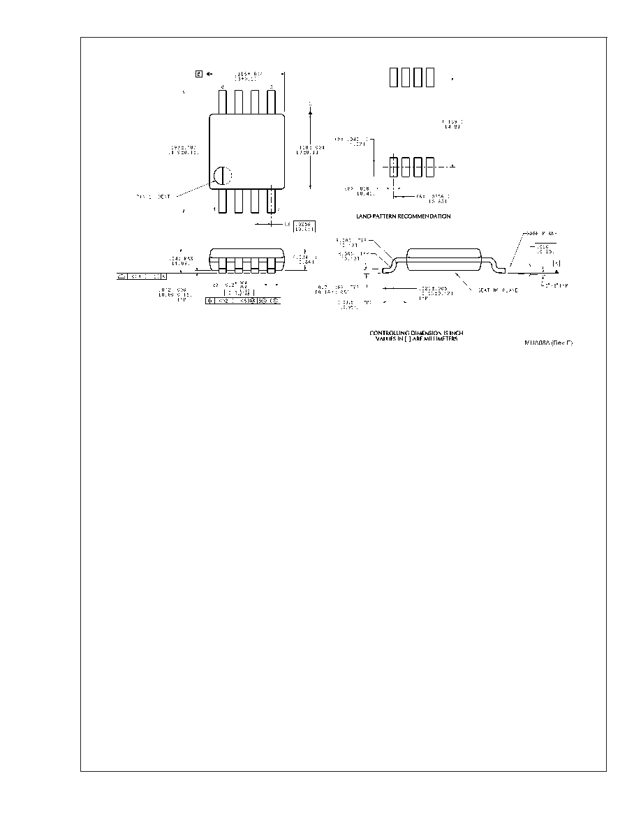
Physical Dimensions
inches (millimeters) unless otherwise noted
8-Lead Mini SO-8 (MM)
NS Package Number MUA08A
For Order Numbers, refer to the table in the "Ordering Information" section of this document.
LM2623
www.national.com
10
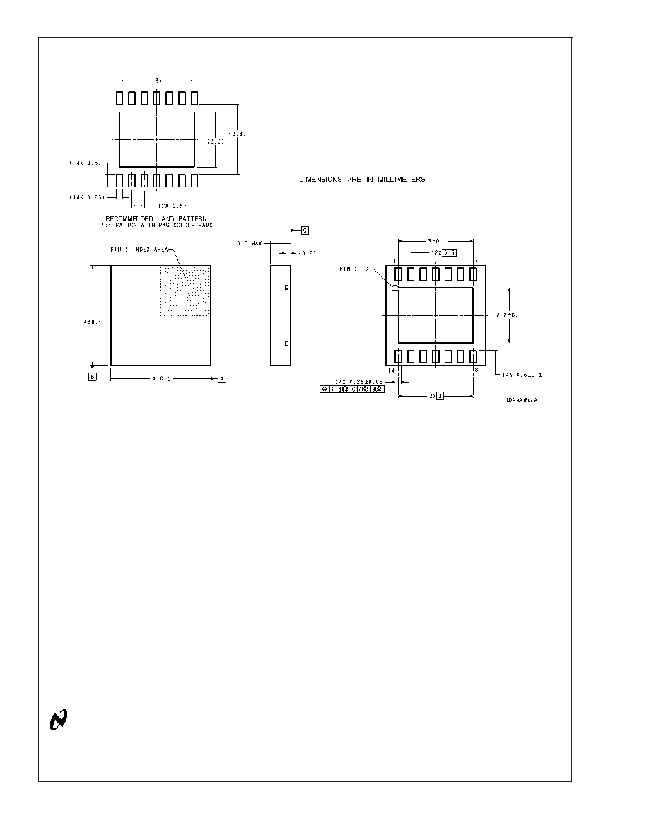
Physical Dimensions
inches (millimeters) unless otherwise noted (Continued)
NS Package Number LDA14A
For Order Numbers, refer to the table in the "Ordering Information" section of this document.
LIFE SUPPORT POLICY
NATIONAL'S PRODUCTS ARE NOT AUTHORIZED FOR USE AS CRITICAL COMPONENTS IN LIFE SUPPORT
DEVICES OR SYSTEMS WITHOUT THE EXPRESS WRITTEN APPROVAL OF THE PRESIDENT AND GENERAL
COUNSEL OF NATIONAL SEMICONDUCTOR CORPORATION. As used herein:
1. Life support devices or systems are devices or
systems which, (a) are intended for surgical implant
into the body, or (b) support or sustain life, and
whose failure to perform when properly used in
accordance with instructions for use provided in the
labeling, can be reasonably expected to result in a
significant injury to the user.
2. A critical component is any component of a life
support device or system whose failure to perform
can be reasonably expected to cause the failure of
the life support device or system, or to affect its
safety or effectiveness.
National Semiconductor
Americas Customer
Support Center
Email: new.feedback@nsc.com
Tel: 1-800-272-9959
National Semiconductor
Europe Customer Support Center
Fax: +49 (0) 180-530 85 86
Email: europe.support@nsc.com
Deutsch Tel: +49 (0) 69 9508 6208
English
Tel: +44 (0) 870 24 0 2171
FranÁais Tel: +33 (0) 1 41 91 8790
National Semiconductor
Asia Pacific Customer
Support Center
Email: ap.support@nsc.com
National Semiconductor
Japan Customer Support Center
Fax: 81-3-5639-7507
Email: jpn.feedback@nsc.com
Tel: 81-3-5639-7560
www.national.com
LM2623
General
Purpose,
Gated
Oscillator
Based,
DC/DC
Boost
Converter
National does not assume any responsibility for use of any circuitry described, no circuit patent licenses are implied and National reserves the right at any time without notice to change said circuitry and specifications.