LM2633
Advanced Two-Phase Synchronous Triple Regulator
Controller for Notebook CPUs
General Description
The LM2633 is a feature-rich IC that combines three regu-
lator controllers - two current mode synchronous buck regu-
lator controllers and a linear regulator controller.
The two switching regulator controllers operate 180∞ out of
phase. This feature reduces the input ripple RMS current,
resulting in a smaller input filter.
The first switching controller (Channel 1) features an Intel
mobile CPU compatible precision 5-bit digital-to-analog con-
verter which programs the output voltage from 0.925V to
2.00V. It is also compatible with the dynamic VID require-
ments. The second switching controller (Channel 2) is ad-
justable between 1.25V to 6.0V.
Use of synchronous rectification and pulse-skip operation at
light load achieves high efficiency over a wide load range.
Fixed-frequency operation can be obtained by disabling the
pulse-skip mode.
Current-mode feedback control assures excellent line and
load regulation and a wide loop bandwidth for good re-
sponse to fast load transient events. Current mode control is
achieved through sensing the Vds of the top FET and thus
an external sense resistor is not necessary.
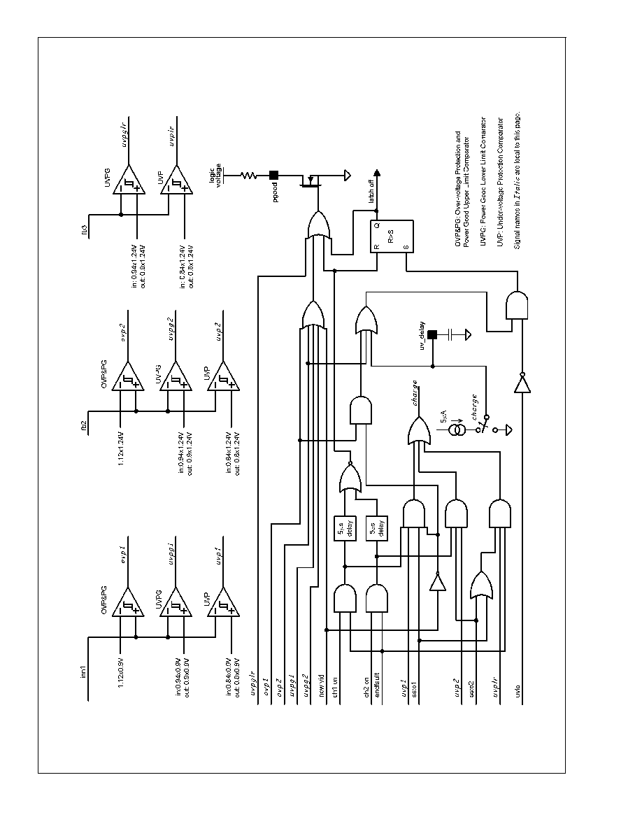
A power good signal is available to indicate the general
health of the output voltages.
A unique feature is the analog soft-start for the switching
controllers is independent of the slew rate of the input volt-
age. This will make the soft start behavior more predictable
and controllable. An internal 5V rail is available externally for
boot-strap circuitry (only) when no 5V is available from other
sources.
Current limit for either of the two switching channels is
achieved through sensing the top FET V
DS
and the value is
adjustable. The two switching controllers have under-voltage
and over-voltage latch protections, and the linear regulator
has under-voltage latch protection. Under-voltage latch can
be disabled or delayed by a programmable amount of time.
The input voltage for the switching channels ranges from 5V
to 30V, which makes possible the choice of different battery
chemistries and options.
Features
GENERAL
n
Three regulated output voltages
n
4.5V to 30V input range
n
Power good function
n
Input under-voltage lockout
n
Thermal shutdown
n
Tiny TSSOP package
SWITCHING SECTION
n
Two channels operating 180∞ out of phase
n
Separate on/off control for each channel
n
Current mode control without sense resistor
n
Skip-mode operation available
n
Adjustable cycle-by-cycle current limit
n
Negative current limit
n
Analog soft start independent of input voltage slew rate
n
Power ground pins separate
n
Output UVP and OVP
n
Programmable output UVP delay
n
250kHz switching frequency (for Vin
<
17V)
n
Channel 1 output from 0.925V to 2.00V
n
±
1.5% DAC accuracy from 0∞C to 125∞C
n
±
1.7% initial tolerance for Channel 2
n
Dynamic VID change ready
n
Power good flags VID changes
n
Channel 2 output from 1.3V to 6.0V
LINEAR SECTION
n
Output voltage adjustable
n
50mA maximum driving current
n
Output UVP
n
±
2% initial tolerance
Applications
n
Power supply for CPUs of notebook PCs that require
the SpeedStep
TM
technique
n
Power supply for information appliances
n
General low voltage DC/DC buck regulators
SpeedStep
TM
is a trademark of Intel Corporation.
August 2001
LM2633
Advanced
T
wo-Phase
Synchronous
T
riple
Regulator
Controller
for
Notebook
CPUs
© 2001 National Semiconductor Corporation
DS200008
www.national.com

Connection Diagram
TOP VIEW
20000801
48-Lead TSSOP (MTD)
Order Number LM2633MTD
See NS Package Number MTD48
Pin Descriptions
FB1 (Pin 1):The feedback input for Channel 1. Connect to
the load directly.
COMP1 (Pin 2): Channel 1 compensation network connec-
tion (connected to the output of the voltage error amplifier).
NC (Pins 3, 14, 15, 20, 26, 28, 37 and 47): No internal
connection.
ON/SS1 (Pin 4): Adding a capacitor to this pin provides a
soft-start function which minimizes inrush current and output
voltage overshoot; A lower than 0.8V input (open-collector
type) at this pin turns off Channel 1; also if both ON/SS1 and
ON/SS2 pins are below 0.8V, the whole IC goes into
shut
down mode. The soft-start capacitor voltage will eventually
be charged to V
IN
or 6V, whichever is lower.
ON/SS2 (Pin 5): Adding a capacitor to this pin provides a
soft-start function which minimizes inrush current and output
voltage overshoot; A lower than 0.8V input (open-collector
type) at this pin turns off Channel 2; also if both ON/SS1 and
ON/SS2 pins are below 0.8V, the whole IC goes into
shut
down mode. The soft-start capacitor voltage will eventually
be charged to V
IN
or 6V, whichever is lower.
VID4-0 (Pins 6-10): Voltage identification code. Each pin
has an internal pull-up. They can accept open collector
compatible 5-bit binary code from the CPU. The code table is
shown in
Table 3.
UV_ DELAY (Pin 11): A capacitor from this pin to ground
adjusts the delay for the output under-voltage lockout.
FPWM (Pin 12): When FPWM is low, pulse-skip mode op-
eration at light load is disabled. The regulator is forced to
operate in constant frequency mode.
PGOOD (Pin 13): : A constant monitor on the output volt-
ages. It indicates the general health of the regulators. For
more information,
see Power Good Truth Table (Table 2) and
Power Good Function in Operation Descriptions.
GND (Pin 16-17): Low-noise analog ground.
G3 (Pin 18): Connect to the base or gate of the linear
regulator pass transistor.
OUT3 (Pin 19): Connect to the output of the linear regulator.
FB3 (Pin 21): The feedback input for the linear regulator,
connected to the center of the external resistor divider.
COMP2 (Pin 22): Channel 2 compensation network connec-
tion (it's the output of the voltage error amplifier).
FB2 (Pin 23): The feedback input for Channel 2. Connect to
the center of the output resistor divider.
SENSE2 (Pin 24): Remote sense pin of Channel 2. This pin
is used for skip-mode operation.
ILIM2 (Pin 25): Current limit threshold setting for Channel 2.
It sinks at a constant 10 µA current. A resistor is connected
between this pin and the top MOSFET drain. The voltage
across this resistor is compared with the V
DS
of the top
MOSFET to determine if an over-current condition has oc-
curred in Channel 2.
KS2 (Pin 27): The Kelvin sense for the drain of the top
MOSFET of Channel 2.
SW2 (Pin 29): Switch-node connection for Channel 2, which
is connected to the source of the top MOSFET.
HDRV2 (Pin 30): Top gate-drive output for Channel 2.
HDRV2 is a floating drive output that rides on SW2 voltage.
CBOOT2 (Pin 31): Bootstrap capacitor connection for Chan-
nel 2 top gate drive. It is the positive supply rail for Channel
2 top gate drive.
VDD2 (Pin 32): The supply rail for Channel 2 bottom gate
drive.
LDRV2 (Pin 33): Bottom gate-drive output for Channel 2.
PGND2 (Pin 34): Power ground for Channel 2.
VIN (Pin 35): The regulator input voltage supply.
VLIN5 (Pin 36): The output of the internal 5V linear regula-
tor. Bypass to the ground with a 1UF ceramic capacitor.
When regulator input voltage is 5V, this pin can be tied to
VIN pin to improve light-load efficiency.
PGND1 (Pin 38-39): Power ground for Channel 1.
LDRV1 (Pin 40-41): Bottom gate-drive output for Channel 1.
VDD1 (Pin 42): The supply rail for the Channel 1 bottom
gate drive.
CBOOT1 (Pin 43): Bootstrap capacitor connection for Chan-
nel 1 top gate drive. It is the positive supply rail for Channel
1 top gate drive.
HDRV1 (Pin 44): Top gate-drive output for Channel 1.
HDRV1 is a floating drive output that rides on SW1 voltage.
SW1 (Pin 45): Switch-node connection for Channel 1, which
is connected to the source of the top MOSFET.
KS1 (Pin 46): The Kelvin sense for the drain of the top
MOSFET of Channel 1.
ILIM1 (Pin 48): Current limit threshold setting for Channel 1.
It sinks at a constant 10 µA current. A resistor is connected
between this pin and the top MOSFET drain. The voltage
across this resistor is compared with the V
DS
of the top
MOSFET to determine if an over-current condition has oc-
curred in Channel 1.
LM2633
www.national.com
2