 | ÐлекÑÑоннÑй компоненÑ: LM2647 | СкаÑаÑÑ:  PDF PDF  ZIP ZIP |
Äîêóìåíòàöèÿ è îïèñàíèÿ www.docs.chipfind.ru
LM2647
Dual Synchronous Buck Regulator Controller
General Description
The LM2647 is an adjustable 200-500kHz dual channel
voltage-mode controlled high-speed synchronous buck
regulator controller ideally suited for battery powered appli-
cations such as laptop and notebook computers. The
LM2647 requires only N-channel FETs for both the upper
and lower positions of each synchronous stage. It features
line feedforward to improve the response to input transients.
At very light loads, the user can choose between the high-
efficiency Pulse-skip mode or the constant frequency
Forced-PWM mode. Lossless current limiting without the use
of external sense resistors is made possible by sensing the
voltage drop across the bottom FET. A unique adaptive duty
cycle clamping technique is incorporated to significantly re-
duce peak currents under abnormal load conditions. The two
independently programmable outputs switch 180° out of
phase (interleaved switching) to reduce the input capacitor
and filter requirements. The input voltage range is 5.5V to
28V while the output voltages are adjustable down to 0.6V.
Standard supervisory and control features include Soft-start,
Power Good, output Under-voltage and Over-voltage protec-
tion, Under-voltage Lockout, Soft-shutdown and Enable.
Features
n
Input voltage range from 5.5V to 28V
n
Synchronous dual-channel Interleaved switching
n
Forced-PWM or Pulse-skip modes
n
Lossless bottom-side FET current sensing
n
Adaptive duty cycle clamping
n
High current N-channel FET drivers
n
Low shutdown supply currents
n
Reference voltage accurate to within
±
1.5%
n
Output voltage adjustable down to 0.6V
n
Power Good flag and Chip Enable
n
Under-voltage lockout
n
Over-voltage/Under-voltage protection
n
Soft-start and Soft-shutdown
n
Switching frequency adjustable 200kHz-500kHz
Applications
n
Notebook Chipset Power Supplies
n
Low Output Voltage High-Efficiency Buck Regulators
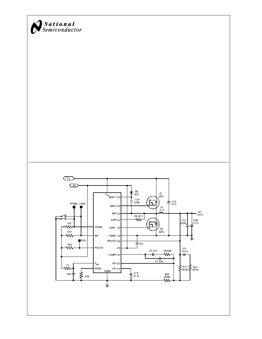
Typical Application (Channel 2 in parenthesis)
20056304
June 2003
Dual
Synchronous
Buck
Regulator
Controller
© 2003 National Semiconductor Corporation
DS200563
www.national.com
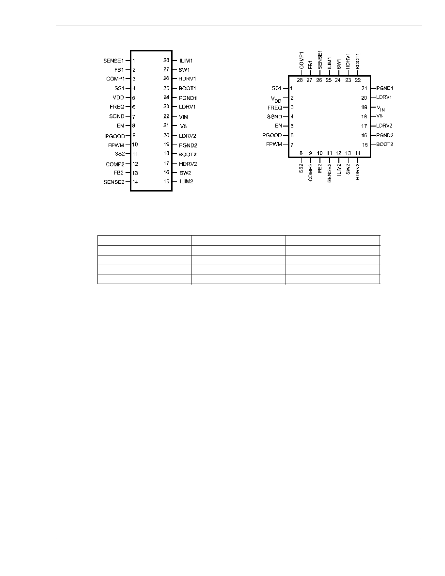
Connection Diagrams
20056302
Top View
28-Lead TSSOP (MTC)
20056303
Top View
28-Lead LLP (LQA)
Ordering Information
Order Number
Package Drawing
Supplied As
LM2647MTC
MTC28
48 Units/Rail
LM2647MTCX
MTC28
2500 Units/13" Reel
LM2647LQ
LQA28A
1000 Units/7" Reel
LM2647LQX
LQA28A
4500 Units/13" Reel
Pin Description
(All pin numbers referred to here correspond to the TSSOP
package)
Pin 1, SENSE1: Output voltage sense pin for Channel 1. It is
tied directly to the output rail. The SENSE pin voltage is used
together with the VIN voltage (on Pin 22) to (internally)
calculate the CCM (continuous conduction mode) duty cycle.
This calculation is used by the IC to set the minimum duty
cycle in the SKIP mode to 85% of the CCM value. It is also
used to set the adaptive duty cycle clamp (see Pin 3). An
internal 20
resistor from the SENSE pin to ground dis-
charges the output capacitor gently (Soft-shutdown) when-
ever Power Not Good is signaled on Pin 9.
Pin 2, FB1: Feedback pin for Channel 1. This is the inverting
input of the error amplifier. The voltage on this pin under
regulation is nominally at 0.6V. A Power Good window on this
pin determines if the output voltage is within regulation limits
(
±
13%). If the voltage (on either channel) falls outside this
window for more than 7µs, Power Not Good is signaled on
the PGOOD pin (Pin 9). Output over-voltage and under-
voltage conditions are also detected by comparing the volt-
age on the Feedback pin with appropriate internal reference
voltage levels. If the voltage exceeds the safe window
(
±
30%) for longer than 7µs, a fault condition is asserted.
Then both the lower FETs are latched ON and the upper
FETs are latched OFF. When single channel operation is
desired, the Feedback pins of both channels should be
connected together, near the IC. All other pins specific to the
unused channel should be left floating (not connected to
each other either).
Pin 3, COMP1: Compensation pin for Channel 1. This is also
the output of the error amplifier of this channel. The voltage
level on this pin is compared with an internally generated
ramp signal to set the duty cycle for normal regulation. Since
the Feedback pin is the inverting input of the same error
amplifier, appropriate control loop compensation compo-
nents are placed between this pin and the Feedback pin.
The COMP pin is internally pulled low during Soft-start so as
to limit the duty cycle. Once Soft-start is completed, the
voltage on this pin can take up the value required to maintain
output regulation. But an internal voltage clamp does not
allow the pin to go much higher than the steady-state re-
quirement. This forms the adaptive duty cycle clamp feature
which serves to limit the maximum allowable duty cycle and
peak currents under sudden overloads. But at the same time
it has enough headroom to permit an adequate response to
step loads within the normal operating range.
Pin 4, SS1: Channel 1 Soft-start pin. A Soft-start capacitor is
placed between this pin and ground. A typical capacitance of
0.1µF is always recommended between this pin and ground.
The IC connects an internal 1.8 k
resistor (R
SS_DCHG
, see
Electrical Characteristics table) between this pin and ground
to discharge any remaining charge on the Soft-start capaci-
tor under several conditions. These conditions include the
initial power-up sequence, start-up by toggling the EN pin,
and also recovery from a fault condition. The purpose is to
bring down the voltage on both the Soft-start pins to below
100mV for obtaining reset. Reset having thus been obtained,
an 11µA current source at this pin charges up the Soft-start
capacitor. The voltage on this pin controls the maximum duty
cycle, and this produces a gradual ramp-up of the output
voltage, thereby preventing large inrush currents into the
LM2647
www.national.com
2

Pin Description
(Continued)
output capacitors. The voltage on this pin finally clamps
close to 5V. This pin is again connected to the internal 115µA
current sink whenever a current limit event is in progress.
This sink current discharges the Soft-start capacitor and
forces the duty cycle low to protect the power components.
When a fault condition is asserted (See Pin 2) the SS pin is
internally connected to ground via the 1.8 k
resistor.
Pin 5, VDD: 5V supply rail for the control and logic sections
of both channels. For normal operation to start, the voltage
on this pin must be brought above 4.5V. Subsequently, the
voltage on this pin (including any ripple component) should
not allowed to fall below 4V for a duration longer than 7µs.
Since this pin is also the supply rail for the internal control
sections, it should be well-decoupled particularly at high
frequencies. A minimum 0.1µF-0.47µF (ceramic) capacitor
should be placed on the component side very close to the IC
with no intervening vias between this capacitor and the
VDD/SGND pins. If the voltage on Pin 5 falls below the lower
UVLO threshold, both upper FETs are latched OFF and
lower FETs latched ON. Power Not Good is then also sig-
naled immediately (on Pin 9). To effect recovery, the EN pin
must be taken below 0.8V and then back above 2V (with
VDD held above 4.5V). Or the voltage on the VDD pin must
be taken below 1.0V and then back again above 4.5V (with
EN pin held above 2V). Normal operation will then resume
assuming that the fault condition has cleared.
Pin 6, FREQ: Frequency adjust pin. The switching frequency
(for both channels) is set by a resistor connected between
this pin and ground. A value of 22.1k
sets the frequency to
300kHz (nominal). If the resistance is increased, the switch-
ing frequency falls. An approximate relationship is that for
every 7.3k
increase (or decrease) in the value of the fre-
quency adjust resistance, the time period (1/f) increases (or
decreases) by about 1µs.
Pin 7, SGND: Signal Ground pin. This is the lower rail for the
control and logic sections of both channels. SGND should be
connected on the PCB to the system ground, which in turn is
connected to PGND1 and PGND2. The layout is important
and the recommendations in the section Layout Guidelines
should be followed.
Pin 8, EN: IC Enable pin. When EN is taken high, both
channels are enabled by means of a Soft-start power-up
sequence (see Pin 4). When EN is brought low, Power Not
Good is signaled within 100ns. This causes Soft-shutdown to
occur (see Pins 1 and 9). The Soft-start capacitor is then
discharged by an internal 1.8k
resistor (R
SS_DCHG
, see
Electrical Characteristics table). But note that when the En-
able pin is toggled, a fault condition is not asserted. There-
fore in this case, the lower FETs are not latched ON, even as
the output voltage ramps down, eventually falling below the
under-voltage threshold. In fact, in this situation, both the
upper and the lower FETs of the two channels are latched
OFF, until the Enable pin is taken high again. If a fault
shutdown has occurred, taking the Enable pin low and then
high again (toggling), resets the internal latches, and the IC
will resume normal switching operation.
Pin 9, PGOOD: Power Good output pin. An open-Drain logic
output that is pulled high with an external pull-up resistor,
indicating that both output voltages are within a pre-defined
Power Good window. Outside this window, the pin is inter-
nally pulled low (Power Not Good signaled) provided the
output error lasts for more than 7µs. But the pin is also pulled
low within 100ns of the Enable pin being taken low, irrespec-
tive of the output voltage level. Note that PGOOD must
always be high before it can respond by going low. So
regulation on both channels must be achieved first. Further,
for fault monitoring to be in place, PGOOD must have been
high prior to occurrence of the fault condition. Note that since
under a fault assertion, the lower FETs are always latched
ON, this will not happen if regulation has not been already
been achieved first. For correct signaling on this pin under
single-channel operation, see description of Pin 2.
Pin 10, FPWM: Logic input for selecting either the Forced
PWM (FPWM) Mode or Pulse-skip Mode (SKIP) for both
channels (together). When the pin is driven high, the IC
operates in the FPWM mode, and when pulled low or left
floating, the SKIP mode is enabled. In FPWM mode, the
lower FET of a given channel is always ON whenever the
upper FET is OFF (except for a narrow shoot-through pro-
tection deadband). This leads to continuous conduction
mode of operation, which has a fixed frequency and (almost)
fixed duty cycle down to very light loads. But this does
reduce efficiency at light loads. The alternative is the SKIP
mode, where the lower FET remains ON only until the volt-
age on the Switch pin (see Pin 27 or Pin 16) is more negative
than 2.2mV (typical). So for example, for a 21m
FET, this
translates to a current threshold of 2.2mV/21m
= 0.1A.
Therefore, if the (instantaneous) inductor current falls below
this value, the lower FET will turn OFF every cycle at this
point (when operated in SKIP mode). This threshold is set by
the zero-cross Comparator in the Block Diagram. Note that if
the inductor current waveform is high enough to be always
above this zero-cross threshold (V
SW_ZERO
, see Table of
Electrical Characteristics), there will be no observable differ-
ence between FPWM and SKIP mode settings (in steady-
state). SKIP mode, when it actually occurs, is clearly a
discontinuous mode of operation. However, note that in con-
ventional discontinuous mode, the duty cycle keeps falling
(towards zero) as the load decreases. But the LM2647 does
not allow the duty cycle to fall by more than 15% of its
original value (at the CCM-DCM boundary). This forces
pulse-skipping, and the average frequency is effectively de-
creased as the load decreases. This mode of operation
improves efficiency at light loads, but the frequency is effec-
tively no longer a constant. Note that a minimum pre-load of
0.1mA should be maintained on the output of each channel
to ensure regulation in SKIP mode. The resistive divider from
output to ground used to set the output voltage could be
designed to serve as part or all of this required pre-load.
Pin 11, SS2: Soft-start pin for Channel 2. See Pin 4.
Pin 12, COMP2: Soft-start pin for Channel 2. See Pin 3.
Pin 13, FB2: Feedback pin for Channel 2. See Pin 2.
Pin 14, SENSE2: Output voltage sense pin for Channel 2.
See Pin 1.
Pin 15, ILIM2: Channel 2 Current Limit pin. When the bottom
FET is ON, a 62µA (typical) current flows out of this pin into
an external current limit setting resistor connected to the
Drain of the lower FET. This is a current source, therefore the
drop across this resistor serves to push the voltage on this
pin to a more positive value. However, the Drain of the lower
FET which is connected to the other side of the same
resistor is trying to go more negative as the load current
increases. At some value of instantaneous current, the volt-
age on this pin will transit from positive to negative. The point
where it is zero is the current limiting condition and is de-
tected by the Current Limit Comparator in the Block Dia-
gram. When current limit condition has been detected, the
next ON-pulse of the upper FET will be omitted. The lower
FET will again be monitored to determine if the current has
fallen below the threshold. If it has, the next ON-pulse will be
LM2647
www.national.com
3

Pin Description
(Continued)
permitted. If not, the upper FET will be turned OFF and will
stay so for several cycles if necessary, until the current
returns to normal. Eventually, if the overcurrent condition
persists, and the upper FET has not been turned ON, the
output will clearly start to fall. Ultimately the output will fall
below the under-voltage threshold, and a fault condition will
be asserted by the IC.
Pin 16, SW2: The Switching node of the buck regulator of
Channel 2. Also serves as the lower rail of the floating driver
of the upper FET.
Pin 17, HDRV2: Gate drive pin for the upper FET of Channel
2 (High-side drive). The top gate driver is interlocked with the
bottom
gate
driver
to
prevent
shoot-through/cross-
conduction.
Pin 18, BOOT2: Bootstrap pin for Channel 2. This is the
upper supply rail for the floating driver of the upper FET. It is
bootstrapped by means of a ceramic capacitor connected to
the channel Switching node. This capacitor is charged up by
the IC to a value of about 5V as derived from the V5 pin (Pin
21).
Pin 19, PGND2: Power Ground pin of Channel 2. This is the
return path for the bottom FET gate drive. Both the PGND's
are to be connected on the PCB to the system ground and
also to the Signal ground (Pin 7) in accordance with the
recommended Layout Guidelines .
Pin 20, LDRV2: Gate drive pin for the Channel 2 bottom FET
(Low-side drive). The bottom gate driver is interlocked with
the
top
gate
driver
to
prevent
shoot-through/cross-
conduction. It is always latched high when a fault condition is
asserted by the IC.
Pin 21, V5: Upper rail of the lower FET drivers of both
channels. Also used to charge up the bootstrap capacitors of
the upper FET drivers. This is connected to an external 5V
supply. The 5V rail may be the same as the rail used to
provide power to the VDD pin (Pin 5), but the VDD pin will
then require to be well-decoupled so that it does not interact
with the V5 pin. A low-pass RC filter consisting of a ceramic
0.1µF capacitor (preferably 0.22µF) and a 10
resistor will
suffice as shown in the Typical Applications circuit.
Pin 22, VIN: The input to both the Buck regulator power
stages. It also is used by the internal ramp generator to
implement the line feedforward feature. The VIN pin is also
used with the SENSE pin voltage to predict the CCM (con-
tinuous conduction mode) duty cycle and to thereby set the
minimum allowed DCM duty cycle to 85% of the CCM value
(in SKIP mode, see Pin 10). This is a high input impedance
pin, drawing only about 100µA (typical) from the input rail.
Pin 23, LDRV1: LDRV pin of Channel 1. See Pin 20.
Pin 24, PGND1: PGND pin for Channel 1.See Pin 19.
Pin 25, BOOT1: Boot pin of Channel 1. See Pin 18.
Pin 26, HDRV1: HDRV pin of Channel 1. See Pin 17.
Pin 27, SW1: SW pin of Channel 1. See Pin 16.
Pin 28, ILIM1: Channel 2 Current Limit pin. See Pin 15.
LM2647
www.national.com
4
Absolute Maximum Ratings
(Note 1)
If Military/Aerospace specified devices are required,
please contact the National Semiconductor Sales Office/
Distributors for availability and specifications.
Voltages from the indicated pins to SGND/PGND unless
otherwise indicated (Note 2):
VIN
30V
V5
7V
VDD
7V
BOOT1, BOOT2
36V
BOOT1 to SW1, BOOT2 to
SW2
7V
SW1, SW2
30V
ILIM1, ILIM2
30V
SENSE1, SENSE2, FB1, FB2
7V
PGOOD
7V
EN
7V
Power Dissipation (T
A
= 25°C)
(Note 3)
1.0W
Junction Temperature
+150°C
ESD Rating (Note 4)
2kV
Ambient Storage Temperature
Range
-65°C to +150°C
Soldering Dwell Time,
Temperature
Wave
Infrared
Vapor Phase
4 sec, 260°C
10 sec, 240°C
75 sec, 219°C
Operating Ratings
(Note 1)
VIN
5.5V to 28V
VDD, V5
4.5V to 5.5V
Junction Temperature
-5°C to +125°C
Electrical Characteristics
Specifications with standard typeface are for T
J
= 25°C, and those with boldface apply over full Operating Junction Tempera-
ture range. VDD = V5 = 5V, V
SGND
= V
PGND
= 0V, VIN = 15V, V
EN
= 3V, R
FADJ
= 22.1K unless otherwise stated. (Note 5)
Symbol
Parameter
Conditions
Min
(Note 6)
Typical
(Note 7)
Max
(Note 6)
Units
Reference
V
FB_REG
FB Pin Voltage at Regualtion
(either FB Pin)
VDD = 4.5V to 5.5V,
VIN = 5.5V to 28V
591
600
609
mV
V
FB
Line Regulation
VDD = 4.5V to 5.5V,
VIN = 5.5V to 28V
0.5
I
FB
FB Pin Current (sourcing)
V
FB
at regulation
20
100
nA
Chip Supply
I
Q_VIN
VIN Quiescent Current
V
FB1
= V
FB2
= 0.7V
100
200
µA
I
SD_VN
VIN Shutdown Current
V
EN
= 0V
0
5
µA
I
Q_VDD
VDD Quiescent Current
V
FB1
= V
FB2
= 0.7V
2.5
4
mA
I
SD_VDD
VDD Shutdown Current
V
EN
= 0V
8
15
µA
I
Q_V5
V5 Normal Operating Current
V
FB1
= V
FB2
= 0.7V
0.3
0.5
mA
V
FB1
= V
FB2
= 0.5V
1
1.5
I
SD_V5
V5 Shutdown Current
V
EN
= 0V
0
5
µA
I
Q_BOOT
BOOT Quiescent Current
V
FB1
= V
FB2
= 0.7V
2
5
µA
V
FB1
= V
FB2
= 0.5V
300
500
I
SD_BOOT
BOOT Shutdown Current
V
EN
= 0V
1
5
µA
V
UVLO
VDD UVLO Threshold
VDD rising from 0V
3.9
4.2
4.5
V
VDD UVLO Hysteresis
VDD = V5 falling from V
UVLO
0.5
0.7
0.9
V
Logic
I
EN
EN Input Current
V
EN
= 0 to 5V
0
µA
V
EN_HI
EN Input Logic High
2
1.8
V
V
EN_LO
EN Input Logic Low
1.3
0.8
V
FPWM Pull-down
V
FPWM
= 2V
100
200
1000
k
V
FPWM_HI
FPWM Input Logic High
2
1.8
V
VFPWM_LO
FPWM Input Logic Low
1.3
0.8
V
LM2647
www.national.com
5
Document Outline