 | –≠–ª–µ–∫—Ç—Ä–æ–Ω–Ω—ã–π –∫–æ–º–ø–æ–Ω–µ–Ω—Ç: LM2651 | –°–∫–∞—á–∞—Ç—å:  PDF PDF  ZIP ZIP |

LM2651
1.5A High Efficiency Synchronous Switching Regulator
General Description
The LM2651 switching regulator provides high efficiency
power conversion over a 100:1 load range (1.5A to 15mA).
This
feature
makes
the
LM2651
an
ideal
fit
in
battery-powered applications that demand long battery life in
both run and standby modes.
Synchronous rectification is used to achieve up to 97% effi-
ciency. At light loads, the LM2651 enters a low power hyster-
etic or "sleep" mode to keep the efficiency high. In many ap-
plications, the efficiency still exceeds 80% at 15mA load. A
shutdown pin is available to disable the LM2651 and reduce
the supply current to less than 10µA.
The LM2651 contains a patented current sensing circuitry for
current mode control. This feature eliminates the external
current sensing resistor required by other current-mode
DC-DC converters.
The LM2651 has a 300 kHz fixed frequency internal oscilla-
tor. The high oscillator frequency allows the use of extremely
small, low profile components.
A programmable soft-start feature limits current surges from
the input power supply at start up and provides a simple
means of sequencing multiple power supplies.
Other protection features include input undervoltage lockout,
current limiting, and thermal shutdown.
Features
n
Ultra high efficiency up to 97%
n
High efficiency over a 1.5A to milliamperes load range
n
4V to 14V input voltage range
n
1.8V, 2.5V, 3.3V, or ADJ output voltage
n
Internal MOSFET switch with low R
DS(on)
of 75m
n
300kHz fixed frequency internal oscillator
n
7µA shutdown current
n
Patented current sensing for current mode control
n
Input undervoltage lockout
n
Adjustable soft-start
n
Current limit and thermal shutdown
n
16-pin TSSOP package
Applications
n
Personal digital assistants (PDAs)
n
Computer peripherals
n
Battery-powered devices
n
Handheld scanners
n
High efficiency 5V conversion
Typical Application
DS100925-15
Efficiency vs Load Current
(V
IN
= 5V, V
OUT
= 3.3V)
DS100925-1
February 2000
LM2651
1.5A
High
Efficiency
Synchronous
Switching
Regulator
© 2000 National Semiconductor Corporation
DS100925
www.national.com
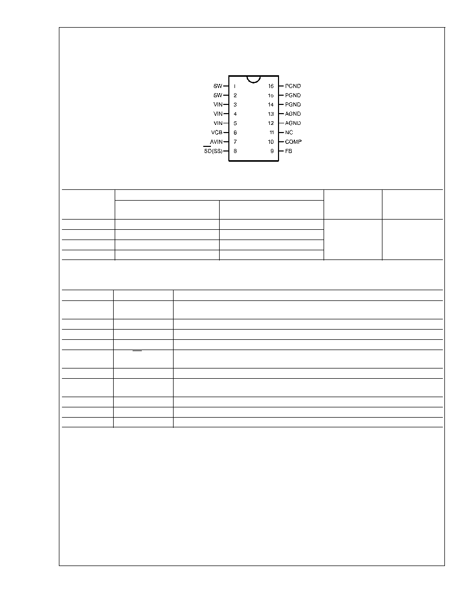
Connection Diagram
Ordering Information
V
OUT
Part Number
Package Type
NSC Package
Drawing
Supplied as 94 Units, Rail
Supplied as 2.5k Units, Tape
and Reel
1.8
LM2651MTC-1.8
LM2651MTCX-1.8
TSSOP-16
MTC16
2.5
LM2651MTC-2.5
LM2651MTCX-2.5
3.3
LM2651MTC-3.3
LM2651MTCX-3.3
ADJ
LM2651MTC-ADJ
LM2651MTCX-ADJ
Pin Description
Pin
Name
Function
1, 2
SW
Switched-node connection, which is connected with the source of the internal high-side
MOSFET.
3-5
VIN
Main power supply pin.
6
VCB
Bootstrap capacitor connection for high-side gate drive.
7
AVIN
Input supply voltage for control and driver circuits.
8
SD(SS)
Shutdown control input, active low. This pin can also function as soft-start control pin. A
capacitor connected from this pin to ground sets the ramp time to full current output.
9
FB
Output voltage feedback input. Connected to the output voltage.
10
COMP
Compensation network connection. Connected to the output of the voltage error
amplifier.
11
NC
No internal connection.
12-13
AGND
Low-noise analog ground.
14-16
PGND
Power ground.
16-Lead TSSOP (MTC)
DS100925-2
LM2651
www.national.com
2

Absolute Maximum Ratings
(Note 1)
If Military/Aerospace specified devices are required,
please contact the National Semiconductor Sales Office/
Distributors for availability and specifications.
Input Voltage
15V
Feedback Pin Voltage
-0.4V
V
FB
5V
Power Dissipation (T
A
=25∞C),
(Note 2)
893 mW
Junction Temperature Range
-40∞C
T
J
+125∞C
Storage Temperature Range
-65∞C to +150∞C
ESD Susceptibility
Human Body Model (Note 3)
1kV
Operating Ratings
(Note 1)
Supply Voltage
4V
V
IN
14V
Electrical Characteristics
Specifications in standard type face are for T
J
= 25∞C and those with boldface
type apply over full operating junction temperature range. V
IN
=10V unless otherwise specified.
LM2651-1.8 System Parameters
Symbol
Parameter
Conditions
Typical
Limit
Units
V
OUT
Output Voltage
I
LOAD
= 900 mA
1.8
1.761/1.719
1.836/1.854
V
V(min)
V(max)
V
OUT
Output Voltage Line
Regulation
V
IN
= 4V to 14V
I
LOAD
= 900 mA
0.2
%
V
OUT
Output Voltage Load
Regulation
I
LOAD
= 10 mA to 1.5A
V
IN
= 5V
1.3
%
V
OUT
Output Voltage Load
Regulation
I
LOAD
= 200 mA to 1.5A
V
IN
= 5V
0.3
%
V
HYST
Sleep Mode Output Voltage
Hysteresis
35
mV
LM2651-2.5 System Parameters
Symbol
Parameter
Conditions
Typical
Limit
Units
V
OUT
Output Voltage
I
LOAD
= 900 mA
2.5
2.43/2.388
2.574/2.575
V
V(min)
V(max)
V
OUT
Output Voltage Line
Regulation
V
IN
= 4V to 12V
I
LOAD
= 900 mA
0.2
%
V
OUT
Output Voltage Load
Regulation
I
LOAD
= 10 mA to 1.5A
V
IN
= 5V
1.3
%
V
OUT
Output Voltage Load
Regulation
I
LOAD
= 200 mA to 1.5A
V
IN
= 5V
0.3
%
V
HYST
Sleep Mode Output Voltage
Hysteresis
48
mV
LM2651-3.3 System Parameters
Symbol
Parameter
Conditions
Typical
Limit
Units
V
OUT
Output Voltage
I
LOAD
= 900 mA
3.3
3.265/3.201
3.379/3.399
V
V(min)
V(max)
V
OUT
Output Voltage Line
Regulation
V
IN
= 4V to 14V
I
LOAD
= 900 mA
0.2
%
V
OUT
Output Voltage Load
Regulation
I
LOAD
= 10 mA to 1.5A
V
IN
= 5V
1.3
%
V
OUT
Output Voltage Load
Regulation
I
LOAD
= 200 mA to 1.5A
V
IN
= 5V
0.3
%
LM2651
www.national.com
3
LM2651-3.3 System Parameters
(Continued)
Symbol
Parameter
Conditions
Typical
Limit
Units
V
HYST
Sleep Mode Output Voltage
Hysteresis
60
mV
LM2651-ADJ System Parameters
(V
OUT
= 2.5V unless otherwise specified)
Symbol
Parameter
Conditions
Typical
Limit
Units
V
FB
Feedback Voltage
I
LOAD
= 900 mA
1.238
1.200
1.263
V
V(min)
V(max)
V
OUT
Output Voltage Line
Regulation
V
IN
= 4V to 14V
I
LOAD
= 900 mA
0.2
%
V
OUT
Output Voltage Load
Regulation
I
LOAD
= 10 mA to 1.5A
V
IN
= 5V
1.3
%
V
OUT
Output Voltage Load
Regulation
I
LOAD
= 200 mA to 1.5A
V
IN
= 5V
0.3
%
V
HYST
Sleep Mode Output Voltage
Hysteresis
24
mV
All Output Voltage Versions
Specifications in standard type face are for T
J
= 25∞C and those with boldface type apply over full operating junction tem-
perature range. V
IN
=10V unless otherwise specified.
Symbol
Parameter
Conditions
Typical
Limit
Units
I
Q
Quiescent Current
1.6
2.0
mA
mA(max)
I
QSD
Quiescent Current in
Shutdown Mode
Shutdown Pin Pulled Low
7
12/20
µA
µA(max)
R
SW(ON)
High-Side or Low-Side
Switch On Resistance
(MOSFET On Resistance +
Bonding Wire Resistance)
I
SWITCH
= 1A
110
m
R
DS(ON)
MOSFET On Resistance
(High-Side or Low-Side)
I
SWITCH
= 1A
75
130
m
m
(max)
I
L
Switch Leakage Current -
High Side
130
nA
Switch Leakage Current -
Low Side
130
nA
V
BOOT
Bootstrap Regulator Voltage
I
BOOT
= 1 mA
6.75
6.45/6.40
6.95/7.00
V
V(min)
V(max)
G
M
Error Amplifier
Transconductance
1250
µmho
V
INUV
V
IN
Undervoltage Lockout
Threshold Voltage
Rising Edge
3.8
3.95
V
V(max)
V
UV-HYST
Hysteresis for the
Undervoltage Lockout
210
mV
I
CL
Switch Current Limit
V
IN
= 5V
2
1.55
2.60
A
A(min)
A(max)
I
SM
Sleep Mode Threshold
Current
V
IN
= 5V
100
mA
A
V
Error Amplifier Voltage Gain
100
V/V
LM2651
www.national.com
4

All Output Voltage Versions
(Continued)
Specifications in standard type face are for T
J
= 25∞C and those with boldface type apply over full operating junction tem-
perature range. V
IN
=10V unless otherwise specified.
Symbol
Parameter
Conditions
Typical
Limit
Units
I
EA_SOURCE
Error Amplifier Source
Current
40
25/15
µA
µA(min)
I
EA_SINK
Error Amplifier Sink Current
65
30
µA
µA(min)
V
EAH
Error Amplifier Output Swing
Upper Limit
2.70
2.50/2.40
V
V(min)
V
EAL
Error Amplifier Output Swing
Lower Limit
1.25
1.35/1.50
V
V(max)
V
D
Body Diode Voltage
I
DIODE
= 1.5A
1
V
f
OSC
Oscillator Frequency
V
IN
= 4V
300
280/255
330/345
kHz
kHz(min)
kHz(max)
D
MAX
Maximum Duty Cycle
V
IN
= 4V
95
92
%
%(min)
I
SS
Soft-Start Current
Voltage at the SS pin = 1.4V
11
7
14
µA
µA(min)
µA(max)
I
SHUTDOWN
Shutdown Pin Current
Shutdown Pin Pulled Low
2.2
0.8/0.5
3.7/4.0
µA
µA(min)
µA(max)
v
SHUTDOWN
Shutdown Pin Threshold
Voltage
Falling Edge
0.6
0.3
0.9
V
V(min)
V(max)
T
SD
Thermal Shutdown
Temperature
165
∞C
T
SD_HYST
Thermal Shutdown
Hysteresis Temperature
25
∞C
Note 1: Absolute maximum ratings indicate limits beyond which damage to the device may occur. Operating ratings indicate conditions for which the device is in-
tended to be functional, but device parameter specifications may not be guaranteed under these conditions. For guaranteed specifications and test conditions, see
the Electrical Characteristics.
Note 2: The maximum allowable power dissipation is calculated by using P
Dmax
= (T
Jmax
- T
A
)/
JA
, where T
Jmax
is the maximum junction temperature, T
A
is the
ambient temperature, and
JA
is the junction-to-ambient thermal resistance of the specified package. The 893 mW rating results from using 150∞C, 25∞C, and
140∞C/W for T
Jmax
, T
A
, and
JA
respectively. A
JA
of 140∞C/W represents the worst-case condition of no heat sinking of the 16-pin TSSOP package. Heat sinking
allows the safe dissipation of more power. The Absolute Maximum power dissipation must be derated by 7.14mW per ∞C above 25∞C ambient. The LM2651 actively
limits its junction temperature to about 165∞C.
Note 3: The human body model is a 100pF capacitor discharged through a 1.5k
resistor into each pin.
Note 4: Typical numbers are at 25∞C and represent the most likely norm.
Note 5: All limits are guaranteed at room temperature (standard typeface) and at temperature extremes (boldface type ). All room temperature limits are 100%
production tested. All limits at temperature extremes are guaranteed via correlation using standard Statistical Quality Control (SQC) methods. All limits are used to
calculate Average Outgoing Quality Level (AOQL).
LM2651
www.national.com
5