
LM2678
SIMPLE SWITCHER
Æ
High Efficiency 5A Step-Down
Voltage Regulator
General Description
The LM2678 series of regulators are monolithic integrated
circuits which provide all of the active functions for a
step-down (buck) switching regulator capable of driving up to
5A loads with excellent line and load regulation characteris-
tics. High efficiency (
>
90%) is obtained through the use of a
low ON-resistance DMOS power switch. The series consists
of fixed output voltages of 3.3V, 5V and 12V and an adjust-
able output version.
The SIMPLE SWITCHER concept provides for a complete
design using a minimum number of external components. A
high fixed frequency oscillator (260KHz) allows the use of
physically smaller sized components. A family of standard in-
ductors for use with the LM2678 are available from several
manufacturers to greatly simplify the design process.
The LM2678 series also has built in thermal shutdown, cur-
rent limiting and an ON/OFF control input that can power
down the regulator to a low 50µA quiescent current standby
condition. The output voltage is guaranteed to a
±
2% toler-
ance. The clock frequency is controlled to within a
±
11% tol-
erance.
Features
n
Efficiency up to 92%
n
Simple and easy to design with (using off-the-shelf
external components)
n
120 m
DMOS output switch
n
3.3V, 5V and 12V fixed output and adjustable (1.2V to
37V ) versions
n
50µA standby current when switched OFF
n
±
2%maximum output tolerance over full line and load
conditions
n
Wide input voltage range: 8V to 40V
n
260 KHz fixed frequency internal oscillator
n
-40 to +125∞C operating junction temperature range
Applications
n
Simple to design, high efficiency (
>
90%) step-down
switching regulators
n
Efficient system pre-regulator for linear voltage
regulators
n
Battery chargers
Typical Application
SIMPLE SWITCHER
Æ
is a registered trademark of National Semiconductor Corporation.
DS100886-3
March 2000
LM2678
SIMPLE
SWITCHER
High
Efficiency
5A
Step-Down
V
oltage
Regulator
© 2000 National Semiconductor Corporation
DS100886
www.national.com
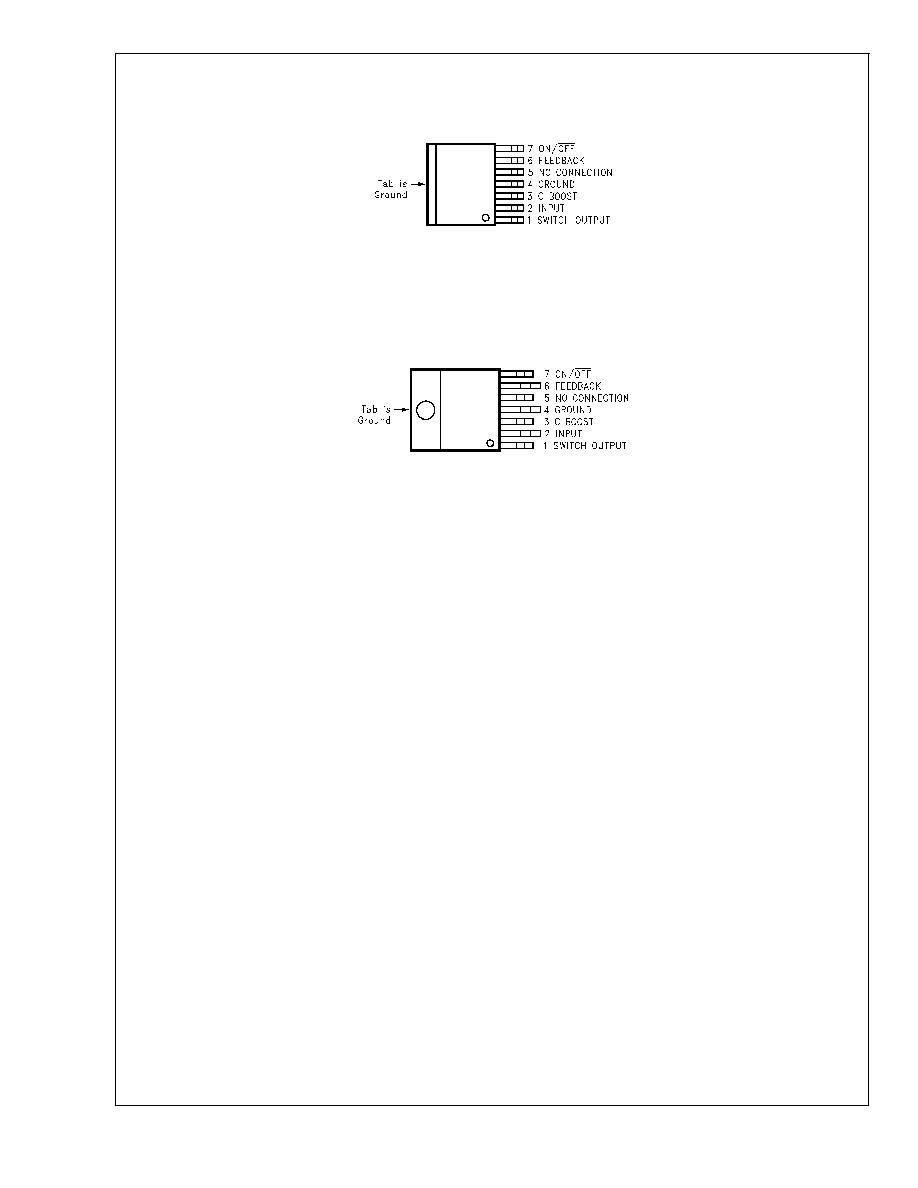
Connection Diagram and Ordering Information
TO-263 Package
Top View
DS100886-1
Order Number
LM2678S-3.3, LM2678S-5.0,
LM2678S-12 or LM2678S-ADJ
See NSC Package Number TS7B
TO-220 Package
Top View
DS100886-2
Order Number
LM2678T-3.3, LM2678T-5.0,
LM2678T-12 or LM2678T-ADJ
See NSC Package Number TA07B
LM2678
www.national.com
2

Absolute Maximum Ratings
(Note 1)
If Military/Aerospace specified devices are required,
please contact the National Semiconductor Sales Office/
Distributors for availability and specifications.
Input Supply Voltage
45V
ON/OFF Pin Voltage
-0.1V to 6V
Switch Voltage to Ground
-1V to V
IN
Boost Pin Voltage
V
SW
+ 8V
Feedback Pin Voltage
-0.3V to 14V
Power Dissipation
Internally Limited
ESD (Note 2)
2 kV
Storage Temperature Range
-65∞C to 150∞C
Soldering Temperature
Wave
4 sec, 260∞C
Infrared
10 sec, 240∞C
Vapor Phase
75 sec, 219∞C
Operating Ratings
Supply Voltage
8V to 40V
Junction Temperature Range (T
J
)
-40∞C to 125∞C
Electrical Characteristics
Limits appearing in bold type face apply over the entire junction temperature
range of operation, -40∞C to 125∞C. Specifications appearing in normal type apply for T
A
= T
J
= 25∞C.
LM2678-3.3
Symbol
Parameter
Conditions
Typical
Min
Max
Units
(Note 3)
(Note 4)
(Note 4)
V
OUT
Output Voltage
V
IN
= 8V to 40V, 100mA
I
OUT
5A
3.3
3.234/3.201
3.366/3.399
V
Efficiency
V
IN
= 12V, I
LOAD
= 5A
82
%
LM2678-5.0
Symbol
Parameter
Conditions
Typical
Min
Max
Units
(Note 3)
(Note 4)
(Note 4)
V
OUT
Output Voltage
V
IN
= 8V to 40V, 100mA
I
OUT
5A
5.0
4.900/4.850
5.100/5.150
V
Efficiency
V
IN
= 12V, I
LOAD
= 5A
84
%
LM2678-12
Symbol
Parameter
Conditions
Typical
Min
Max
Units
(Note 3)
(Note 4)
(Note 4)
V
OUT
Output Voltage
V
IN
= 15V to 40V, 100mA
I
OUT
5A
12
11.76/11.64
12.24/12.36
V
Efficiency
V
IN
= 24V, I
LOAD
= 5A
92
%
LM2678-ADJ
Symbol
Parameter
Conditions
Typ
Min
Max
Units
(Note 3)
(Note 4)
(Note 4)
V
FB
Feedback
Voltage
V
IN
= 8V to 40V, 100mA
I
OUT
5A
V
OUT
Programmed for 5V
1.21
1.186/1.174
1.234/1.246
V
Efficiency
V
IN
= 12V, I
LOAD
= 5A
84
%
LM2678
www.national.com
3
All Output Voltage Versions
Electrical Characteristics
Limits appearing in bold type face apply over the entire junction temperature range of operation, -40∞C to 125∞C.
Specifications appearing in normal type apply for T
A
= T
J
= 25∞C. Unless otherwise specified V
IN
=12V for the 3.3V, 5V and
Adjustable versions and V
IN
=24V for the 12V version.
Symbol
Parameter
Conditions
Typ
Min
Max
Units
DEVICE PARAMETERS
I
Q
Quiescent
Current
V
FEEDBACK
= 8V
4.2
6
mA
For 3.3V, 5.0V, and ADJ Versions
V
FEEDBACK
= 15V
For 12V Versions
I
STBY
Standby
Quiescent
Current
ON/OFF Pin = 0V
50
100/150
µA
I
CL
Current Limit
7
6.1/5.75
8.3/8.75
A
I
L
Output
Leakage
Current
V
IN
= 40V, ON/OFF Pin = 0V
V
SWITCH
= 0V
V
SWITCH
= -1V
1
6
200
15
µA
mA
R
DS(ON)
Switch
On-Resistance
I
SWITCH
= 5A
0.12
0.14/0.225
f
O
Oscillator
Frequency
Measured at Switch Pin
260
225
280
kHz
D
Duty Cycle
Maximum Duty Cycle
91
%
Minimum Duty Cycle
0
%
I
BIAS
Feedback Bias
Current
V
FEEDBACK
= 1.3V
ADJ Version Only
85
nA
V
ON/OFF
ON/OFF
Threshold
Voltage
1.4
0.8
2.0
V
I
ON/OFF
ON/OFF Input
Current
ON/OFF Input = 0V
20
45
µA
JA
Thermal
Resistance
T Package, Junction to Ambient
65
(Note 5)
JA
T Package, Junction to Ambient
45
(Note 6)
JC
T Package, Junction to Case
2
JA
S Package, Junction to Ambient
56
∞C/W
(Note 7)
JA
S Package, Junction to Ambient
35
(Note 8)
JA
S Package, Junction to Ambient
26
(Note 9)
JC
S Package, Junction to Case
2
++
Note 1: Absolute Maximum Ratings are limits beyond which damage to the device may occur. Operating Ratings indicate conditions under which of the device is
guaranteed. Operating Ratings do not imply guaranteed performance limits. For guaranteed performance limits and associated test condition, see the electrical Char-
acteristics tables.
Note 2: ESD was applied using the human-body model, a 100pF capacitor discharged through a 1.5 k
resistor into each pin.
Note 3: Typical values are determined with T
A
= T
J
= 25∞C and represent the most likely norm.
Note 4: All limits are guaranteed at room temperature (standard type face) and at temperature extremes (bold type face). All room temperature limits are 100%
tested during production with T
A
= T
J
= 25∞C. All limits at temperature extremes are guaranteed via correlation using standard standard Quality Control (SQC) meth-
ods. All limits are used to calculate Average Outgoing Quality Level (AOQL).
Note 5: Junction to ambient thermal resistance (no external heat sink) for the 7 lead TO-220 package mounted vertically, with
1
/
2
inch leads in a socket, or on a PC
board with minimum copper area.
Note 6: Junction to ambient thermal resistance (no external heat sink) for the 7 lead TO-220 package mounted vertically, with
1
/
2
inch leads soldered to a PC board
containing approximately 4 square inches of (1 oz.) copper area surrounding the leads.
LM2678
www.national.com
4

(Continued)
Note 7: Junction to ambient thermal resistance for the 7 lead TO-263 mounted horizontally against a PC board area of 0.136 square inches (the same size as the
TO-263 package) of 1 oz. (0.0014 in. thick) copper.
Note 8: Junction to ambient thermal resistance for the 7 lead TO-263 mounted horizontally against a PC board area of 0.4896 square inches (3.6 times the area of
the TO-263 package) of 1 oz. (0.0014 in. thick) copper.
Note 9: Junction to ambient thermal resistance for the 7 lead TO-263 mounted horizontally against a PC board copper area of 1.0064 square inches (7.4 times the
area of the TO-263 package) of 1 oz. (0.0014 in. thick) copper. Additional copper area will reduce thermal resistance further. See the thermal model in Switchers Made
Simple
Æ
software.
LM2678
www.national.com
5
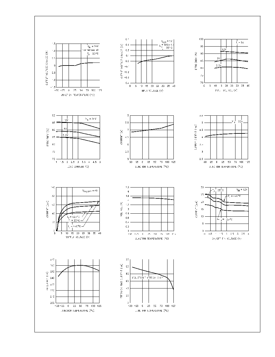
Typical Performance Characteristics
Normalized
Output Voltage
DS100886-9
Line Regulation
DS100886-10
Efficiency vs Input Voltage
DS100886-11
Efficiency vs I
LOAD
DS100886-12
Switch Current Limit
DS100886-4
Operating Quiescent Current
DS100886-5
Standby Quiescent Current
DS100886-40
ON/OFF Threshold Voltage
DS100886-13
ON/OFF Pin Current (Sourcing)
DS100886-14
Switching Frequency
DS100886-15
Feedback Pin Bias Current
DS100886-16
LM2678
www.national.com
6
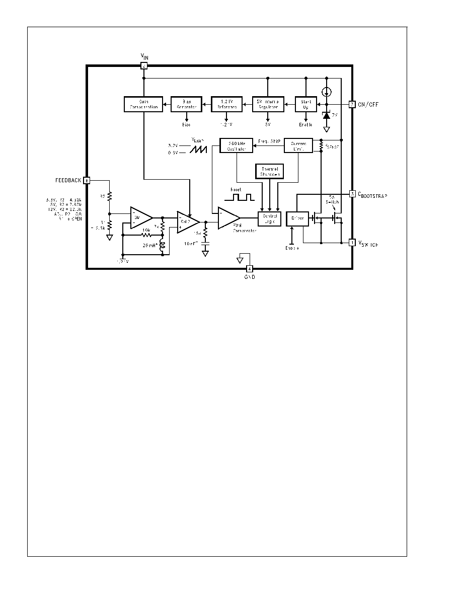
Block Diagram
DS100886-6
* Active Inductor Patent Number 5,514,947
Active Capacitor Patent Number 5,382,918
LM2678
www.national.com
7

Typical Performance Characteristics
Continuous Mode Switching Waveforms
V
IN
= 20V, V
OUT
= 5V, I
LOAD
= 5A
L = 10 µH, C
OUT
= 400 µF, C
OUT
ESR = 13 m
DS100886-17
A: V
SW
Pin Voltage, 10 V/div.
B: Inductor Current, 2 A/div
C: Output Ripple Voltage, 20 mV/div AC-Coupled
Horizontal Time Base: 1 µs/div
Discontinuous Mode Switching Waveforms
V
IN
= 20V, V
OUT
= 5V, I
LOAD
= 500 mA
L = 10 µH, C
OUT
= 400 µF, C
OUT
ESR = 13 m
DS100886-18
A: V
SW
Pin Voltage, 10 V/div.
B: Inductor Current, 1 A/div
C: Output Ripple Voltage, 20 mV/div AC-Coupled
Horizontal Time Base: 1 µs//iv
Load Transient Response for Continuous Mode
V
IN
= 20V, V
OUT
= 5V
L = 10 µH, C
OUT
= 400 µF, C
OUT
ESR = 13 m
DS100886-19
A: Output Voltage, 100 mV//div, AC-Coupled.
B: Load Current: 500 mA to 5A Load Pulse
Horizontal Time Base: 100 µs/div
Load Transient Response for Discontinuous Mode
V
IN
= 20V, V
OUT
= 5V,
L = 10 µH, C
OUT
= 400 µF, C
OUT
ESR = 13 m
DS100886-20
A: Output Voltage, 100 mV/div, AC-Coupled.
B: Load Current: 200 mA to 3A Load Pulse
Horizontal Time Base: 200 µs/div
LM2678
www.national.com
8
Application Hints
The LM2678 provides all of the active functions required for
a step-down (buck) switching regulator. The internal power
switch is a DMOS power MOSFET to provide power supply
designs with high current capability, up to 5A, and highly ef-
ficient operation.
The LM2678 is part of the
SIMPLE SWITCHER family of
power converters. A complete design uses a minimum num-
ber
of
external
components,
which
have
been
pre-determined from a variety of manufacturers. Using either
this data sheet or a design software program called
LM267X
Made Simple (version 2.0) a complete switching power sup-
ply can be designed quickly. The software is provided free of
charge and can be downloaded from National Semiconduc-
tor's Internet site located at http://www.national.com.
PIN 1 - Switch Output
This is the output of a power MOSFET switch connected di-
rectly to the input voltage. The switch provides energy to an
inductor, an output capacitor and the load circuitry under
control of an internal pulse-width-modulator (PWM). The
PWM controller is internally clocked by a fixed 260KHz oscil-
lator. In a standard step-down application the duty cycle
(Time ON/Time OFF) of the power switch is proportional to
the ratio of the power supply output voltage to the input volt-
age. The voltage on pin 1 switches between Vin (switch ON)
and below ground by the voltage drop of the external Schot-
tky diode (switch OFF).
PIN 2 - Input
The input voltage for the power supply is connected to pin 2.
In addition to providing energy to the load the input voltage
also provides bias for the internal circuitry of the LM2678.
For guaranteed performance the input voltage must be in the
range of 8V to 40V. For best performance of the power sup-
ply the input pin should always be bypassed with an input ca-
pacitor located close to pin 2.
PIN 3 - C Boost
A capacitor must be connected from pin 3 to the switch out-
put, pin 1. This capacitor boosts the gate drive to the internal
MOSFET above Vin to fully turn it ON. This minimizes con-
duction losses in the power switch to maintain high effi-
ciency. The recommended value for C Boost is 0.01µF.
PIN 4 - Ground
This is the ground reference connection for all components
in the power supply. In fast-switching, high-current applica-
tions such as those implemented with the LM2678, it is rec-
ommended that a broad ground plane be used to minimize
signal coupling throughout the circuit
PIN 5 - No Connection
PIN 6 - Feedback
This is the input to a two-stage high gain amplifier, which
drives the PWM controller. It is necessary to connect pin 6 to
the actual output of the power supply to set the dc output
voltage. For the fixed output devices (3.3V, 5V and 12V out-
puts), a direct wire connection to the output is all that is re-
quired as internal gain setting resistors are provided inside
the LM2678. For the adjustable output version two external
resistors are required to set the dc output voltage. For stable
operation of the power supply it is important to prevent cou-
pling of any inductor flux to the feedback input.
PIN 7 - ON/OFF
This input provides an electrical ON/OFF control of the
power supply. Connecting this pin to ground or to any volt-
age less than 0.8V will completely turn OFF the regulator.
The current drain from the input supply when OFF is only
50µA. Pin 7 has an internal pull-up current source of approxi-
mately 20µA and a protection clamp zener diode of 7V to
ground. When electrically driving the ON/OFF pin the high
voltage level for the ON condition should not exceed the 6V
absolute maximum limit. When ON/OFF control is not re-
quired pin 7 should be left open circuited.
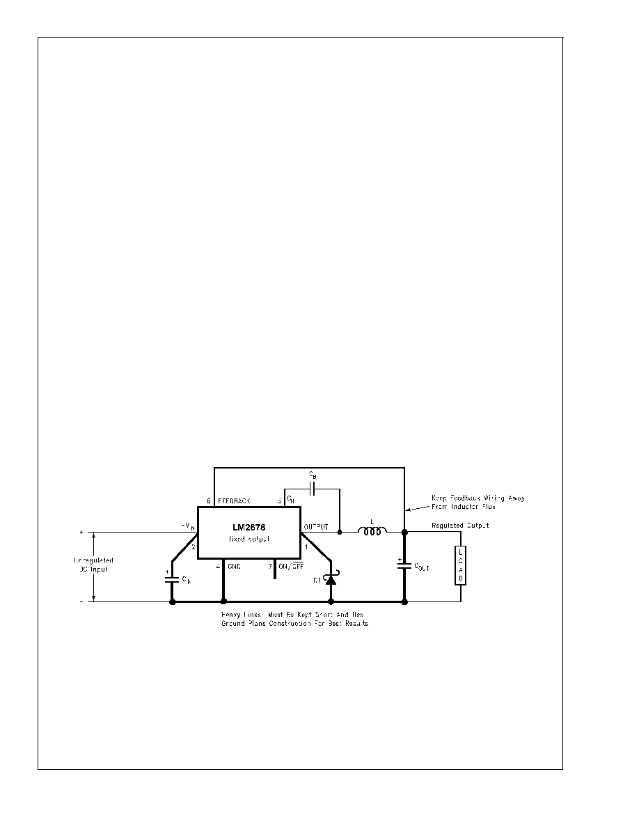
DESIGN CONSIDERATIONS
DS100886-7
FIGURE 1. Basic circuit for fixed output voltage applications.
LM2678
www.national.com
9
Application Hints
(Continued)
Power supply design using the LM2678 is greatly simplified
by using recommended external components. A wide range
of inductors, capacitors and Schottky diodes from several
manufacturers have been evaluated for use in designs that
cover the full range of capabilities (input voltage, output volt-
age and load current) of the LM2678. A simple design proce-
dure using nomographs and component tables provided in
this data sheet leads to a working design with very little ef-
fort. Alternatively, the design software,
LM267X Made
Simple (version 2.0), can also be used to provide instant
component selection, circuit performance calculations for
evaluation, a bill of materials component list and a circuit
schematic.
The individual components from the various manufacturers
called out for use are still just a small sample of the vast ar-
ray of components available in the industry. While these
components are recommended, they are not exclusively the
only components for use in a design. After a close compari-
son of component specifications, equivalent devices from
other manufacturers could be substituted for use in an appli-
cation.
Important considerations for each external component and
an explanation of how the nomographs and selection tables
were developed follows.
INDUCTOR
The inductor is the key component in a switching regulator.
For efficiency the inductor stores energy during the switch
ON time and then transfers energy to the load while the
switch is OFF.
Nomographs are used to select the inductance value re-
quired for a given set of operating conditions. The nomo-
graphs assume that the circuit is operating in continuous
mode (the current flowing through the inductor never falls to
zero). The magnitude of inductance is selected to maintain a
maximum ripple current of 30% of the maximum load cur-
rent. If the ripple current exceeds this 30% limit the next
larger value is selected.
The inductors offered have been specifically manufactured
to provide proper operation under all operating conditions of
input and output voltage and load current. Several part types
are offered for a given amount of inductance. Both surface
mount and through-hole devices are available. The inductors
from each of the three manufacturers have unique charac-
teristics.
Renco: ferrite stick core inductors; benefits are typically low-
est cost and can withstand ripple and transient peak currents
above the rated value. These inductors have an external
magnetic field, which may generate EMI.
Pulse Engineering: powdered iron toroid core inductors;
these also can withstand higher than rated currents and, be-
ing toroid inductors, will have low EMI.
Coilcraft: ferrite drum core inductors; these are the smallest
physical size inductors and are available only as surface
mount components. These inductors also generate EMI but
less than stick inductors.
OUTPUT CAPACITOR
The output capacitor acts to smooth the dc output voltage
and also provides energy storage. Selection of an output ca-
pacitor, with an associated equivalent series resistance
(ESR), impacts both the amount of output ripple voltage and
stability of the control loop.
The output ripple voltage of the power supply is the product
of the capacitor ESR and the inductor ripple current. The ca-
pacitor types recommended in the tables were selected for
having low ESR ratings.
In addition, both surface mount tantalum capacitors and
through-hole aluminum electrolytic capacitors are offered as
solutions.
Impacting frequency stability of the overall control loop, the
output capacitance, in conjunction with the inductor, creates
a double pole inside the feedback loop. In addition the ca-
pacitance and the ESR value create a zero. These fre-
quency response effects together with the internal frequency
compensation circuitry of the LM2678 modify the gain and
phase shift of the closed loop system.
As a general rule for stable switching regulator circuits it is
desired to have the unity gain bandwidth of the circuit to be
limited to no more than one-sixth of the controller switching
frequency. With the fixed 260KHz switching frequency of the
LM2678, the output capacitor is selected to provide a unity
gain bandwidth of 40KHz maximum. Each recommended ca-
pacitor value has been chosen to achieve this result.
DS100886-8
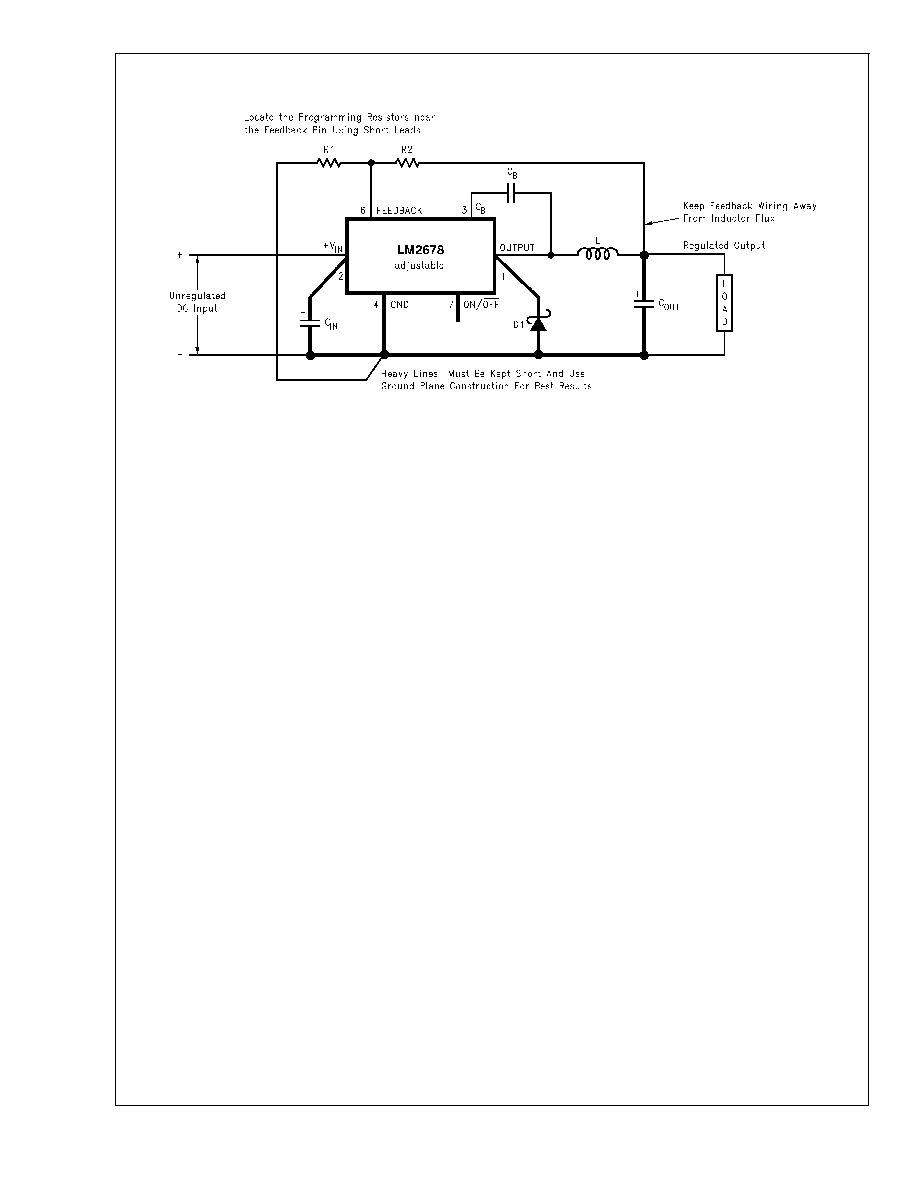
FIGURE 2. Basic circuit for adjustable output voltage applications
LM2678
www.national.com
10

Application Hints
(Continued)
In some cases multiple capacitors are required either to re-
duce the ESR of the output capacitor, to minimize output
ripple (a ripple voltage of 1% of Vout or less is the assumed
performance condition), or to increase the output capaci-
tance to reduce the closed loop unity gain bandwidth (to less
than 40KHz). When parallel combinations of capacitors are
required it has been assumed that each capacitor is the ex-
act same part type.
The RMS current and working voltage (WV) ratings of the
output capacitor are also important considerations. In a typi-
cal step-down switching regulator, the inductor ripple current
(set to be no more than 30% of the maximum load current by
the inductor selection) is the current that flows through the
output capacitor. The capacitor RMS current rating must be
greater than this ripple current. The voltage rating of the out-
put capacitor should be greater than 1.3 times the maximum
output voltage of the power supply. If operation of the system
at elevated temperatures is required, the capacitor voltage
rating may be de-rated to less than the nominal room tem-
perature rating. Careful inspection of the manufacturer's
specification for de-rating of working voltage with tempera-
ture is important.
INPUT CAPACITOR
Fast changing currents in high current switching regulators
place a significant dynamic load on the unregulated power
source. An input capacitor helps to provide additional current
to the power supply as well as smooth out input voltage
variations.
Like the output capacitor, the key specifications for the input
capacitor are RMS current rating and working voltage. The
RMS current flowing through the input capacitor is equal to
one-half of the maximum dc load current so the capacitor
should be rated to handle this. Paralleling multiple capacitors
proportionally increases the current rating of the total capaci-
tance. The voltage rating should also be selected to be 1.3
times the maximum input voltage. Depending on the unregu-
lated input power source, under light load conditions the
maximum input voltage could be significantly higher than
normal operation and should be considered when selecting
an input capacitor.
The input capacitor should be placed very close to the input
pin of the LM2678. Due to relative high current operation
with fast transient changes, the series inductance of input
connecting wires or PCB traces can create ringing signals at
the input terminal which could possibly propagate to the out-
put or other parts of the circuitry. It may be necessary in
some designs to add a small valued (0.1µF to 0.47µF) ce-
ramic type capacitor in parallel with the input capacitor to
prevent or minimize any ringing.
CATCH DIODE
When the power switch in the LM2678 turns OFF, the current
through the inductor continues to flow. The path for this cur-
rent is through the diode connected between the switch out-
put and ground. This forward biased diode clamps the switch
output to a voltage less than ground. This negative voltage
must be greater than -1V so a low voltage drop (particularly
at high current levels) Schottky diode is recommended. Total
efficiency of the entire power supply is significantly impacted
by the power lost in the output catch diode. The average cur-
rent through the catch diode is dependent on the switch duty
cycle (D) and is equal to the load current times (1-D). Use of
a diode rated for much higher current than is required by the
actual application helps to minimize the voltage drop and
power loss in the diode.
During the switch ON time the diode will be reversed biased
by the input voltage. The reverse voltage rating of the diode
should be at least 1.3 times greater than the maximum input
voltage.
BOOST CAPACITOR
The boost capacitor creates a voltage used to overdrive the
gate of the internal power MOSFET. This improves efficiency
by minimizing the on resistance of the switch and associated
power loss. For all applications it is recommended to use a
0.01µF/50V ceramic capacitor.
SIMPLE DESIGN PROCEDURE
Using the nomographs and tables in this data sheet (or use
the available design software at http://www.national.com) a
complete step-down regulator can be designed in a few
simple steps.
Step 1: Define the power supply operating conditions:
Required output voltage
Maximum DC input voltage
Maximum output load current
Step 2: Set the output voltage by selecting a fixed output
LM2678 (3.3V, 5V or 12V applications) or determine the re-
quired feedback resistors for use with the adjustable
LM2678-ADJ
Step 3: Determine the inductor required by using one of the
four nomographs, Figure 3 through Figure 6. Table 1 pro-
vides a specific manufacturer and part number for the induc-
tor.
Step 4: Using Table 3 (fixed output voltage) or Table 6 (ad-
justable output voltage), determine the output capacitance
required for stable operation. Table 2 provides the specific
capacitor type from the manufacturer of choice.
Step 5: Determine an input capacitor from Table 4 for fixed
output voltage applications. Use Table 2 to find the specific
capacitor type. For adjustable output circuits select a capaci-
tor from Table 2 with a sufficient working voltage (WV) rating
greater than Vin max, and an rms current rating greater than
one-half the maximum load current (2 or more capacitors in
parallel may be required).
Step 6: Select a diode from Table 5. The current rating of the
diode must be greater than I load max and the Reverse Volt-
age rating must be greater than Vin max.
Step 7: Include a 0.01µF/50V capacitor for Cboost in the de-
sign.
FIXED OUTPUT VOLTAGE DESIGN EXAMPLE
A system logic power supply bus of 3.3V is to be generated
from a wall adapter which provides an unregulated DC volt-
age of 13V to 16V. The maximum load current is 4A.
Through-hole components are preferred.
Step 1: Operating conditions are:
Vout = 3.3V
Vin max = 16V
Iload max = 4A
Step 2: Select an LM2678T-3.3. The output voltage will have
a tolerance of
±
2% at room temperature and
±
3% over the full operating
temperature range.
Step 3: Use the nomograph for the 3.3V device ,
Figure 3.
The intersection of the 16V horizontal line (V
in
max) and the
4A vertical line (I
load
max) indicates that L46, a 15µH induc-
tor, is required.
From Table 1, L46 in a through-hole component is available
from Renco with part number RL-1283-15-43.
LM2678
www.national.com
11
Application Hints
(Continued)
Step 4: Use Table 3 to determine an output capacitor. With a
3.3V output and a 15µH inductor there are four through-hole
output capacitor solutions with the number of same type ca-
pacitors to be paralleled and an identifying capacitor code
given. Table 2 provides the actual capacitor characteristics.
Any of the following choices will work in the circuit:
2 x 220µF/10V Sanyo OS-CON (code C5)
2 x 820µF/16V Sanyo MV-GX (code C5)
1 x 3900µF/10V Nichicon PL (code C7)
2 x 560µF/35V Panasonic HFQ (code C5)
Step 5: Use Table 4 to select an input capacitor. With 3.3V
output and 15µH there are three through-hole solutions.
These capacitors provide a sufficient voltage rating and an
rms current rating greater than 2A (1/2 I
load
max). Again us-
ing Table 2 for specific component characteristics the follow-
ing choices are suitable:
2 x 680µF/63V Sanyo MV-GX (code C13)
1 x 1200µF/63V Nichicon PL (code C25)
1 x 1500µF/63V Panasonic HFQ (code C16)
Step 6: From Table 5 a 5A or more Schottky diode must be
selected. For through-hole components only 40V rated di-
odes are indicated and 4 part types are suitable:
1N5825
MBR745
80SQ045
6TQ045
Step 7: A 0.01µF capacitor will be used for Cboost.
ADJUSTABLE OUTPUT DESIGN EXAMPLE
In this example it is desired to convert the voltage from a two
battery automotive power supply (voltage range of 20V to
28V, typical in large truck applications) to the 14.8VDC alter-
nator supply typically used to power electronic equipment
from single battery 12V vehicle systems. The load current re-
quired is 3.5A maximum. It is also desired to implement the
power supply with all surface mount components.
Step 1: Operating conditions are:
Vout = 14.8V
Vin max = 28V
Iload max = 3.5A
Step 2: Select an LM2678S-ADJ. To set the output voltage
to 14.9V two resistors need to be chosen (R1 and R2 in
Fig-
ure 2). For the adjustable device the output voltage is set by
the following relationship:
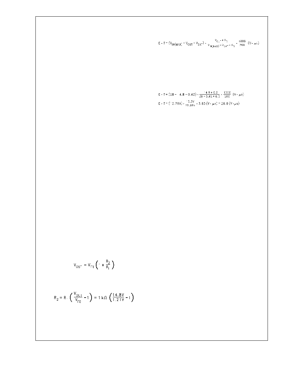
Where V
FB
is the feedback voltage of typically 1.21V.
A recommended value to use for R1 is 1K. In this example
then R2 is determined to be:
R2 = 11.23K
The closest standard 1% tolerance value to use is 11.3K
This will set the nominal output voltage to 14.88V which is
within 0.5% of the target value.
Step 3: To use the nomograph for the adjustable device,
Fig-
ure
6,
requires
a
calculation
of
the
inductor
Volt
∑
microsecond constant (E
∑
T expressed in V
∑
µS) from
the following formula:
where V
SAT
is the voltage drop across the internal power
switch which is R
ds(ON)
times I
load
. In this example this would
be typically 0.12
x 3.5A or 0.42V and V
D
is the voltage drop
across the forward bisased Schottky diode, typically 0.5V.
The switching frequency of 260KHz is the nominal value to
use to estimate the ON time of the switch during which en-
ergy is stored in the inductor.
For this example E
∑
T is found to be:
Using
Figure 6, the intersection of 27V
∑
µS horizontally and
the 3.5A vertical line (I
load
max) indicates that L48 , a 47µH
inductor, or L49, a 33µH inductor could be used. Either in-
ductor will be suitable, but for this example selecting the
larger inductance will result in lower ripple current.
From Table 1, L48 in a surface mount component is available
from Pulse Engineering with part number P0848.
Step 4: Use Table 6 to determine an output capacitor. With a
14.8V output the 12.5 to 15V row is used and with a 47µH in-
ductor there are three surface mount output capacitor solu-
tions. Table 2 provides the actual capacitor characteristics
based on the C Code number. Any of the following choices
can be used:
1 x 33µF/20V AVX TPS (code C6)
1 x 47µF/20V Sprague 594 (code C8)
1 x 47µF/20V Kemet T495 (code C8)
Important Note: When using the adjustable device in low
voltage applications (less than 3V output), if the nomograph,
Figure 6, selects an inductance of 22µH or less, Table 6 does
not provide an output capacitor solution. With these condi-
tions the number of output capacitors required for stable op-
eration becomes impractical. It is recommended to use ei-
ther a 33µH or 47µH inductor and the output capacitors from
Table 6.
Step 5: An input capacitor for this example will require at
least a 35V WV rating with an rms current rating of 1.75A
(1/2 Iout max). From Table 2 it can be seen that C12, a
33µF/35V
capacitor
from
Sprague,
has
the
highest
voltage/current rating of the surface mount components and
that two of these capacitor in parallel will be adquate.
Step 6: From Table 5 a 5A or more Schottky diode must be
selected. For surface mount diodes with a margin of safety
on the voltage rating one of two diodes can be used:
MBRD1545CT
6TQ045S
Step 7: A 0.01µF capacitor will be used for Cboost.
LM2678
www.national.com
12

Application Hints
(Continued)
INDUCTOR VALUE SELECTION GUIDES (For Continuous Mode Operation)
DS100886-21
FIGURE 3. LM2678-3.3
DS100886-22
FIGURE 4. LM2678-5.0
DS100886-23
FIGURE 5. LM2678-12
DS100886-24
FIGURE 6. LM2678-ADJ
LM2678
www.national.com
13

Application Hints
(Continued)
TABLE 1. Inductor Manufacturer Part Numbers
Inductor
Reference
Number
Inductance
(µH)
Current
(A)
Renco
Pulse Engineering
Coilcraft
Through Hole
Surface
Mount
Through
Hole
Surface
Mount
Surface Mount
L23
33
1.35
RL-5471-7
RL1500-33
PE-53823
PE-53823S
DO3316-333
L24
22
1.65
RL-1283-22-43
RL1500-22
PE-53824
PE-53824S
DO3316-223
L25
15
2.00
RL-1283-15-43
RL1500-15
PE-53825
PE-53825S
DO3316-153
L29
100
1.41
RL-5471-4
RL-6050-100
PE-53829
PE-53829S
DO5022P-104
L30
68
1.71
RL-5471-5
RL6050-68
PE-53830
PE-53830S
DO5022P-683
L31
47
2.06
RL-5471-6
RL6050-47
PE-53831
PE-53831S
DO5022P-473
L32
33
2.46
RL-5471-7
RL6050-33
PE-53932
PE-53932S
DO5022P-333
L33
22
3.02
RL-1283-22-43
RL6050-22
PE-53933
PE-53933S
DO5022P-223
L34
15
3.65
RL-1283-15-43
--
PE-53934
PE-53934S
DO5022P-153
L38
68
2.97
RL-5472-2
--
PE-54038
PE-54038S
--
L39
47
3.57
RL-5472-3
--
PE-54039
PE-54039S
--
L40
33
4.26
RL-1283-33-43
--
PE-54040
PE-54040S
--
L41
22
5.22
RL-1283-22-43
--
PE-54041
P0841
--
L44
68
3.45
RL-5473-3
--
PE-54044
--
--
L45
10
4.47
RL-1283-10-43
--
--
P0845
DO5022P-103HC
L46
15
5.60
RL-1283-15-43
--
--
P0846
DO5022P-153HC
L47
10
5.66
RL-1283-10-43
--
--
P0847
DO5022P-103HC
L48
47
5.61
RL-1282-47-43
--
--
P0848
--
L49
33
5.61
RL-1282-33-43
--
--
P0849
--
Inductor Manufacturer Contact Numbers
Coilcraft
Phone
(800) 322-2645
FAX
(708) 639-1469
Coilcraft, Europe
Phone
+44 1236 730 595
FAX
+44 1236 730 627
Pulse Engineering
Phone
(619) 674-8100
FAX
(619) 674-8262
Pulse Engineering,
Phone
+353 93 24 107
Europe
FAX
+353 93 24 459
Renco Electronics
Phone
(800) 645-5828
FAX
(516) 586-5562
LM2678
www.national.com
14
Application Hints
(Continued)
TABLE 2. Input and Output Capacitor Codes
Capacitor
Reference
Code
Surface Mount
AVX TPS Series
Sprague 594D Series
Kemet T495 Series
C
(µF)
WV
(V)
Irms
(A)
C
(µF)
WV
(V)
Irms
(A)
C
(µF)
WV
(V)
Irms
(A)
C1
330
6.3
1.15
120
6.3
1.1
100
6.3
0.82
C2
100
10
1.1
220
6.3
1.4
220
6.3
1.1
C3
220
10
1.15
68
10
1.05
330
6.3
1.1
C4
47
16
0.89
150
10
1.35
100
10
1.1
C5
100
16
1.15
47
16
1
150
10
1.1
C6
33
20
0.77
100
16
1.3
220
10
1.1
C7
68
20
0.94
180
16
1.95
33
20
0.78
C8
22
25
0.77
47
20
1.15
47
20
0.94
C9
10
35
0.63
33
25
1.05
68
20
0.94
C10
22
35
0.66
68
25
1.6
10
35
0.63
C11
15
35
0.75
22
35
0.63
C12
33
35
1
4.7
50
0.66
C13
15
50
0.9
LM2678
www.national.com
15
Application Hints
(Continued)
Input and Output Capacitor Codes (continued)
Capacitor
Reference
Code
Through Hole
Sanyo OS-CON SA
Series
Sanyo MV-GX Series
Nichicon PL Series
Panasonic HFQ Series
C (µF)
WV
(V)
Irms
(A)
C
(µF)
WV
(V)
Irms
(A)
C
(µF)
WV
(V)
Irms
(A)
C
(µF)
WV
(V)
Irms
(A)
C1
47
6.3
1
1000
6.3
0.8
680
10
0.8
82
35
0.4
C2
150
6.3
1.95
270
16
0.6
820
10
0.98
120
35
0.44
C3
330
6.3
2.45
470
16
0.75
1000
10
1.06
220
35
0.76
C4
100
10
1.87
560
16
0.95
1200
10
1.28
330
35
1.01
C5
220
10
2.36
820
16
1.25
2200
10
1.71
560
35
1.4
C6
33
16
0.96
1000
16
1.3
3300
10
2.18
820
35
1.62
C7
100
16
1.92
150
35
0.65
3900
10
2.36
1000
35
1.73
C8
150
16
2.28
470
35
1.3
6800
10
2.68
2200
35
2.8
C9
100
20
2.25
680
35
1.4
180
16
0.41
56
50
0.36
C10
47
25
2.09
1000
35
1.7
270
16
0.55
100
50
0.5
C11
220
63
0.76
470
16
0.77
220
50
0.92
C12
470
63
1.2
680
16
1.02
470
50
1.44
C13
680
63
1.5
820
16
1.22
560
50
1.68
C14
1000
63
1.75
1800
16
1.88
1200
50
2.22
C15
220
25
0.63
330
63
1.42
C16
220
35
0.79
1500
63
2.51
C17
560
35
1.43
C18
2200
35
2.68
C19
150
50
0.82
C20
220
50
1.04
C21
330
50
1.3
C22
100
63
0.75
C23
390
63
1.62
C24
820
63
2.22
C25
1200
63
2.51
Capacitor Manufacturer Contact Numbers
Nichicon
Phone
(847) 843-7500
FAX
(847) 843-2798
Panasonic
Phone
(714) 373-7857
FAX
(714) 373-7102
AVX
Phone
(845) 448-9411
FAX
(845) 448-1943
Sprague/Vishay
Phone
(207) 324-4140
FAX
(207) 324-7223
Sanyo
Phone
(619) 661-6322
FAX
(619) 661-1055
Kemet
Phone
(864) 963-6300
FAX
(864) 963-6521
LM2678
www.national.com
16

Application Hints
(Continued)
TABLE 3. Output Capacitors for Fixed Output Voltage Application
Output
Voltage
(V)
Inductance
(µH)
Surface Mount
AVX TPS Series
Sprague 594D
Series
Kemet T495 Series
No.
C Code
No.
C Code
No.
C Code
3.3
10
5
C1
5
C1
5
C2
15
4
C1
4
C1
4
C3
22
3
C2
2
C7
3
C4
33
1
C1
2
C7
3
C4
5
10
4
C2
4
C6
4
C4
15
3
C3
2
C7
3
C5
22
3
C2
2
C7
3
C4
33
2
C2
2
C3
2
C4
47
2
C2
1
C7
2
C4
12
10
4
C5
3
C6
5
C9
15
3
C5
2
C7
4
C9
22
2
C5
2
C6
3
C8
33
2
C5
1
C7
3
C8
47
2
C4
1
C6
2
C8
68
1
C5
1
C5
2
C7
100
1
C4
1
C5
1
C8
Output
Voltage
(V)
Inductance
(µH)
Through Hole
Sanyo OS-CON SA
Series
Sanyo MV-GX
Series
Nichicon PL Series
Panasonic HFQ
Series
No.
C Code
No.
C Code
No.
C Code
No.
C Code
3.3
10
2
C5
2
C6
1
C8
2
C6
15
2
C5
2
C5
1
C7
2
C5
22
1
C5
1
C10
1
C5
1
C7
33
1
C5
1
C10
1
C5
1
C7
5
10
2
C4
2
C5
1
C6
2
C5
15
1
C5
1
C10
1
C5
1
C7
22
1
C5
1
C9
1
C5
1
C5
33
1
C4
1
C5
1
C4
1
C4
47
1
C4
1
C4
1
C2
2
C4
12
10
2
C7
1
C10
1
C14
2
C4
15
1
C8
1
C6
1
C17
1
C5
22
1
C7
1
C5
1
C13
1
C5
33
1
C7
1
C4
1
C12
1
C4
47
1
C7
1
C3
1
C11
1
C3
68
1
C6
1
C2
1
C10
1
C3
100
1
C6
1
C2
1
C9
1
C1
No. represents the number of identical capacitor types to be connected in parallel
C Code indicates the Capacitor Reference number in Table 2 for identifying the specific component from the manufacturer.
LM2678
www.national.com
17
Application Hints
(Continued)
TABLE 4. Input Capacitors for Fixed Output Voltage Application
(Assumes worst case maximum input voltage and load current for a given inductance value)
Output
Voltage
(V)
Inductance
(µH)
Surface Mount
AVX TPS Series
Sprague 594D
Series
Kemet T495 Series
No.
C Code
No.
C Code
No.
C Code
3.3
10
3
C7
2
C10
3
C9
15
*
*
3
C13
4
C12
22
*
*
2
C13
3
C12
33
*
*
2
C13
3
C12
5
10
3
C4
2
C6
3
C9
15
4
C9
3
C12
4
C10
22
*
*
3
C13
4
C12
33
*
*
2
C13
3
C12
47
*
*
1
C13
2
C12
12
10
4
C9
2
C10
4
C10
15
4
C8
2
C10
4
C10
22
4
C9
3
C12
4
C10
33
*
*
3
C13
4
C12
47
*
*
2
C13
3
C12
68
*
*
2
C13
2
C12
100
*
*
1
C13
2
C12
Output
Voltage
(V)
Inductance
(µH)
Through Hole
Sanyo OS-CON SA
Series
Sanyo MV-GX
Series
Nichicon PL Series
Panasonic HFQ
Series
No.
C Code
No.
C Code
No.
C Code
No.
C Code
3.3
10
2
C9
2
C8
1
C18
1
C8
15
*
*
2
C13
1
C25
1
C16
22
*
*
1
C14
1
C24
1
C16
33
*
*
1
C14
1
C24
1
C16
5
10
2
C7
2
C8
1
C25
1
C8
15
*
*
2
C8
1
C25
1
C8
22
*
*
2
C13
1
C25
1
C16
33
*
*
1
C14
1
C23
1
C13
47
*
*
1
C12
1
C19
1
C11
12
10
2
C10
2
C8
1
C18
1
C8
15
2
C10
2
C8
1
C18
1
C8
22
*
*
2
C8
1
C18
1
C8
33
*
*
2
C12
1
C24
1
C14
47
*
*
1
C14
1
C23
1
C13
68
*
*
1
C13
1
C21
1
C15
100
*
*
1
C11
1
C22
1
C11
*
Check voltage rating of capacitors to be greater than application input voltage.
No. represents the number of identical capacitor types to be connected in parallel
C Code indicates the Capacitor Reference number in Table 2 for identifying the specific component from the manufacturer.
LM2678
www.national.com
18
Application Hints
(Continued)
TABLE 5. Schottky Diode Selection Table
Reverse
Voltage
(V)
Surface Mount
Through Hole
3A
5A or More
3A
5A or
More
20V
SK32
1N5820
SR302
30V
SK33
MBRD835L
1N5821
30WQ03F
31DQ03
40V
SK34
MBRD1545CT
1N5822
1N5825
30BQ040
6TQ045S
MBR340
MBR745
30WQ04F
31DQ04
80SQ045
MBRS340
SR403
6TQ045
MBRD340
50V or
More
SK35
MBR350
30WQ05F
31DQ05
SR305
Diode Manufacturer Contact Numbers
International Rectifier
Phone
(310) 322-3331
FAX
(310) 322-3332
Motorola
Phone
(800) 521-6274
FAX
(602) 244-6609
General
Semiconductor
Phone
(516) 847-3000
FAX
(516) 847-3236
Diodes, Inc.
Phone
(805) 446-4800
FAX
(805) 446-4850
LM2678
www.national.com
19

Application Hints
(Continued)
TABLE 6. Output Capacitors for Adjustable Output Voltage Applications
Output Voltage
(V)
Inductance
(µH)
Surface Mount
AVX TPS Series
Sprague 594D
Series
Kemet T495 Series
No.
C Code
No.
C Code
No.
C Code
1.21 to 2.50
33
*
7
C1
6
C2
7
C3
47
*
5
C1
4
C2
5
C3
2.5 to 3.75
33
*
4
C1
3
C2
4
C3
47
*
3
C1
2
C2
3
C3
3.75 to 5
22
4
C1
3
C2
4
C3
33
3
C1
2
C2
3
C3
47
2
C1
2
C2
2
C3
5 to 6.25
22
3
C2
3
C3
3
C4
33
2
C2
2
C3
2
C4
47
2
C2
2
C3
2
C4
68
1
C2
1
C3
1
C4
6.25 to 7.5
22
3
C2
1
C4
3
C4
33
2
C2
1
C3
2
C4
47
1
C3
1
C4
1
C6
68
1
C2
1
C3
1
C4
7.5 to 10
33
2
C5
1
C6
2
C8
47
1
C5
1
C6
2
C8
68
1
C5
1
C6
1
C8
100
1
C4
1
C5
1
C8
10 to 12.5
33
1
C5
1
C6
2
C8
47
1
C5
1
C6
2
C8
68
1
C5
1
C6
1
C8
100
1
C5
1
C6
1
C8
12.5 to 15
33
1
C6
1
C8
1
C8
47
1
C6
1
C8
1
C8
68
1
C6
1
C8
1
C8
100
1
C6
1
C8
1
C8
15 to 20
33
1
C8
1
C10
2
C10
47
1
C8
1
C9
2
C10
68
1
C8
1
C9
2
C10
100
1
C8
1
C9
1
C10
20 to 30
33
2
C9
2
C11
2
C11
47
1
C10
1
C12
1
C11
68
1
C9
1
C12
1
C11
100
1
C9
1
C12
1
C11
30 to 37
10
4
C13
8
C12
15
3
C13
5
C12
22
No Values Available
2
C13
4
C12
33
1
C13
3
C12
47
1
C13
2
C12
68
1
C13
2
C12
LM2678
www.national.com
20

Application Hints
(Continued)
Output Capacitors for Adjustable Output Voltage Applications (continued)
Output Voltage
(V)
Inductance
(µH)
Through Hole
Sanyo OS-CON SA
Series
Sanyo MV-GX
Series
Nichicon PL Series
Panasonic HFQ
Series
No.
C Code
No.
C Code
No.
C Code
No.
C Code
1.21 to 2.50
33
*
2
C3
5
C1
5
C3
3
C
47
*
2
C2
4
C1
3
C3
2
C5
2.5 to 3.75
33
*
1
C3
3
C1
3
C1
2
C5
47
*
1
C2
2
C1
2
C3
1
C5
3.75 to 5
22
1
C3
3
C1
3
C1
2
C5
33
1
C2
2
C1
2
C1
1
C5
47
1
C2
2
C1
1
C3
1
C5
5 to 6.25
22
1
C5
2
C6
2
C3
2
C5
33
1
C4
1
C6
2
C1
1
C5
47
1
C4
1
C6
1
C3
1
C5
68
1
C4
1
C6
1
C1
1
C5
6.25 to 7.5
22
1
C5
1
C6
2
C1
1
C5
33
1
C4
1
C6
1
C3
1
C5
47
1
C4
1
C6
1
C1
1
C5
68
1
C4
1
C2
1
C1
1
C5
7.5 to 10
33
1
C7
1
C6
1
C14
1
C5
47
1
C7
1
C6
1
C14
1
C5
68
1
C7
1
C2
1
C14
1
C2
100
1
C7
1
C2
1
C14
1
C2
10 to 12.5
33
1
C7
1
C6
1
C14
1
C5
47
1
C7
1
C2
1
C14
1
C5
68
1
C7
1
C2
1
C9
1
C2
100
1
C7
1
C2
1
C9
1
C2
12.5 to 15
33
1
C9
1
C10
1
C15
1
C2
47
1
C9
1
C10
1
C15
1
C2
68
1
C9
1
C10
1
C15
1
C2
100
1
C9
1
C10
1
C15
1
C2
15 to 20
33
1
C10
1
C7
1
C15
1
C2
47
1
C10
1
C7
1
C15
1
C2
68
1
C10
1
C7
1
C15
1
C2
100
1
C10
1
C7
1
C15
1
C2
20 to 30
33
1
C7
1
C16
1
C2
47
No Values
1
C7
1
C16
1
C2
68
Available
1
C7
1
C16
1
C2
100
1
C7
1
C16
1
C2
30 to 37
10
1
C12
1
C20
1
C10
15
1
C11
1
C20
1
C11
22
No Values
1
C11
1
C20
1
C10
33
Available
1
C11
1
C20
1
C10
47
1
C11
1
C20
1
C10
68
1
C11
1
C20
1
C10
* Set to a higher value for a practical design solution. See Applications Hints section
No. represents the number of identical capacitor types to be connected in parallel
C Code indicates the Capacitor Reference number in Table 2 for identifying the specific component from the manufacturer.
LM2678
www.national.com
21
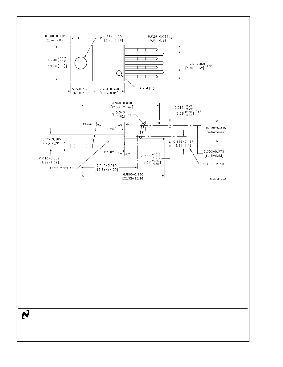
Physical Dimensions
inches (millimeters) unless otherwise noted
TO-263 Surface Mount Power Package
Order Number LM2678S-3.3, LM2678S-5.0,
LM2678S-12 or LM2678S-ADJ
NS Package Number TS7B
LM2678
www.national.com
22
Physical Dimensions
inches (millimeters) unless otherwise noted (Continued)
LIFE SUPPORT POLICY
NATIONAL'S PRODUCTS ARE NOT AUTHORIZED FOR USE AS CRITICAL COMPONENTS IN LIFE SUPPORT
DEVICES OR SYSTEMS WITHOUT THE EXPRESS WRITTEN APPROVAL OF THE PRESIDENT AND GENERAL
COUNSEL OF NATIONAL SEMICONDUCTOR CORPORATION. As used herein:
1. Life support devices or systems are devices or
systems which, (a) are intended for surgical implant
into the body, or (b) support or sustain life, and
whose failure to perform when properly used in
accordance with instructions for use provided in the
labeling, can be reasonably expected to result in a
significant injury to the user.
2. A critical component is any component of a life
support device or system whose failure to perform
can be reasonably expected to cause the failure of
the life support device or system, or to affect its
safety or effectiveness.
National Semiconductor
Corporation
Americas
Tel: 1-800-272-9959
Fax: 1-800-737-7018
Email: support@nsc.com
National Semiconductor
Europe
Fax: +49 (0) 180-530 85 86
Email: europe.support@nsc.com
Deutsch Tel: +49 (0) 69 9508 6208
English
Tel: +44 (0) 870 24 0 2171
FranÁais Tel: +33 (0) 1 41 91 8790
National Semiconductor
Asia Pacific Customer
Response Group
Tel: 65-2544466
Fax: 65-2504466
Email: ap.support@nsc.com
National Semiconductor
Japan Ltd.
Tel: 81-3-5639-7560
Fax: 81-3-5639-7507
www.national.com
TO-220 Power Package
Order Number LM2678T-3.3, LM2678T-5.0,
LM2678T-12 or LM2678T-ADJ
NS Package Number TA07B
LM2678
SIMPLE
SWITCHER
High
Efficiency
5A
Step-Down
V
oltage
Regulator
National does not assume any responsibility for use of any circuitry described, no circuit patent licenses are implied and National reserves the right at any time without notice to change said circuitry and specifications.