 | –≠–ª–µ–∫—Ç—Ä–æ–Ω–Ω—ã–π –∫–æ–º–ø–æ–Ω–µ–Ω—Ç: LM2682MMX | –°–∫–∞—á–∞—Ç—å:  PDF PDF  ZIP ZIP |

LM2682
Switched Capacitor Voltage Doubling Inverter
General Description
The LM2682 is a CMOS charge-pump voltage inverter ca-
pable of converting positive voltage in the range of +2.0V to
+5.5V to the corresponding doubled negative voltage of
-4.0V to -11.0V respectively. The LM2682 uses three low
cost capacitors to provide 10 mA of output current without
the cost, size, and EMI related to inductor based circuits.
With an operating current of only 150 µA and an operating ef-
ficiency greater than 90% with most loads, the LM2682 pro-
vides ideal performance for battery powered systems. The
LM2682 offers a switching frequency of 6 kHz.
Features
n
Inverts then doubles input supply voltage
n
Small MSOP-8 package (mini SO-8) and SO-8 package
n
90
typical output impedance
n
94% typical power efficiency at 10 mA
Applications
n
LCD contrast biasing
n
GaAs power amplifier biasing
n
Interface power supplies
n
Handheld instrumentation
n
Laptop computers and PDAs
Typical Operating Circuit and Pin Configuration
Ordering Information
Order Number
Package
Package Number
Package Marking
Supplied As
LM2682MM
MSOP-8
MUA08A
S11A
Tape and Reel (1000 units/reel)
LM2682MMX
MSOP-8
MUA08A
S11A
Tape and Reel (3500 units/reel)
LM2682M
SO-8
M08A
LM2682M
Rail (95 units/rail)
LM2682MX
SO-8
M08A
LM2682M
Tape and Reel (2500 units/reel)
DS100997-1
8-Pin MSOP
or 8-Pin SOIC
DS100997-2
November 1999
LM2682
Switched
Capacitor
V
oltage
Doubling
Inverter
© 1999 National Semiconductor Corporation
DS100997
www.national.com

Absolute Maximum Ratings
(Note 1)
If Military/Aerospace specified devices are required,
please contact the National Semiconductor Sales Office/
Distributors for availability and specifications.
Input Voltage (V
IN
)
+5.8V
V
IN
dV/dT
1V/µsec
V
OUT
-11.6V
V
OUT
Short-Circuit Duration
Continuous
Storage Temperature
-65∞C to +150∞C
Lead Temperature Soldering
+300∞C
Power Dissipation (Note 2)
MSOP-8
300 mW
SO-8
470 mW
T
JMAX
+150∞C
Operating Ratings
ESD Susceptibility (Note 3)
Human Body Model
Machine Model
2 kV
200V
Ambient Temp. Range
-40∞C to +85∞C
Junction Temp. Range
-40∞C to +125∞C
LM2682
Electrical Characteristics
V
IN
= 5V and C
1
= C
2
= C
3
= 3.3µF unless otherwise specified. Limits with bold
typeface apply over the full operating ambient temperature range, -40∞C to +85∞C, limits with standard typeface apply for T
A
= 25∞C.
Symbol
Parameter
Conditions
Min
Typical
(Note 4)
Max
Units
V
IN
Supply Voltage Range
R
L
= 2 k
2.0
5.5
V
I
IN
Supply Current
Open Circuit, No Load
150
300
400
µA
R
OUT
V
OUT
Source Resistance
I
L
= 10 mA
90
150
200
I
L
=5 mA, V
IN
=2 V
110
250
f
OSC
Oscillator Frequency
(Note 5)
12
30
kHz
f
SW
Switching Frequency
(Note 5)
6
15
kHz
POWER
Power Efficiency
R
L
= 2k (Note 6)
90
93
%
VOLTAGE
Voltage Conversion Efficiency
99.9
%
Note 1: Absolute Maximum Ratings are those values beyond which damage to the device may occur. Operating Ratings indicate conditions for which the device is
intended to be functional, but do not guarantee specific performance limits. For guaranteed specifications and test conditions, see the Electrical Characteristics.
Note 2: The maximum power dissipation must be de-rated at elevated temperatures (only needed for T
A
>
85∞C) and is limited by T
JMAX
(maximum junction tempera-
ture),
J-A
(junction to ambient thermal resistance) and T
A
(ambient temperature).
J-A
is 140∞C/W for the SO-8 package and 220∞C/W for the MSOP-8 package. The
maximum power dissipation at any temperature is:
PDiss
MAX
= (T
JMAX
- T
A
)/
J-A
up to the value listed in the Absolute Maximum Ratings.
Note 3: The human body model is a 100 pF capacitor discharged through a 1.5 k
resistor into each pin. The machine model is a 200pF capacitor discharged di-
rectly into each pin.
Note 4: Typical numbers are at 25∞C and represent the most likely norm.
Note 5: The output switches operate at one half of the oscillator frequency, f
OSC
= 2f
SW
.
Note 6: The minimum specification is guaranteed by design and is not tested.
Pin Description
Pin Number
Symbol
Description
1
C
1
-
Capacitor C
1
negative terminal
2
C
2
+
Capacitor C
2
positive terminal
3
C
2
-
Capacitor C
2
negative terminal
4
V
OUT
Negative output voltage (-2V
IN
)
5
GND
Device ground
6
V
IN
Power supply voltage
7
C
1
+
Capacitor C
1
positive terminal
8
NC
No Connection
LM2682
www.national.com
2

Typical Performance Charactistics
V
IN
= 5V and T
A
= 25∞C unless otherwise noted.
Output Resistance vs Input Voltage
DS100997-6
Output Voltage vs Load Current
DS100997-7
Supply Current vs Input Voltage
DS100997-8
Output Resistance vs Temperature
DS100997-9
Output Voltage Ripple vs Load Current
DS100997-10
LM2682
www.national.com
3
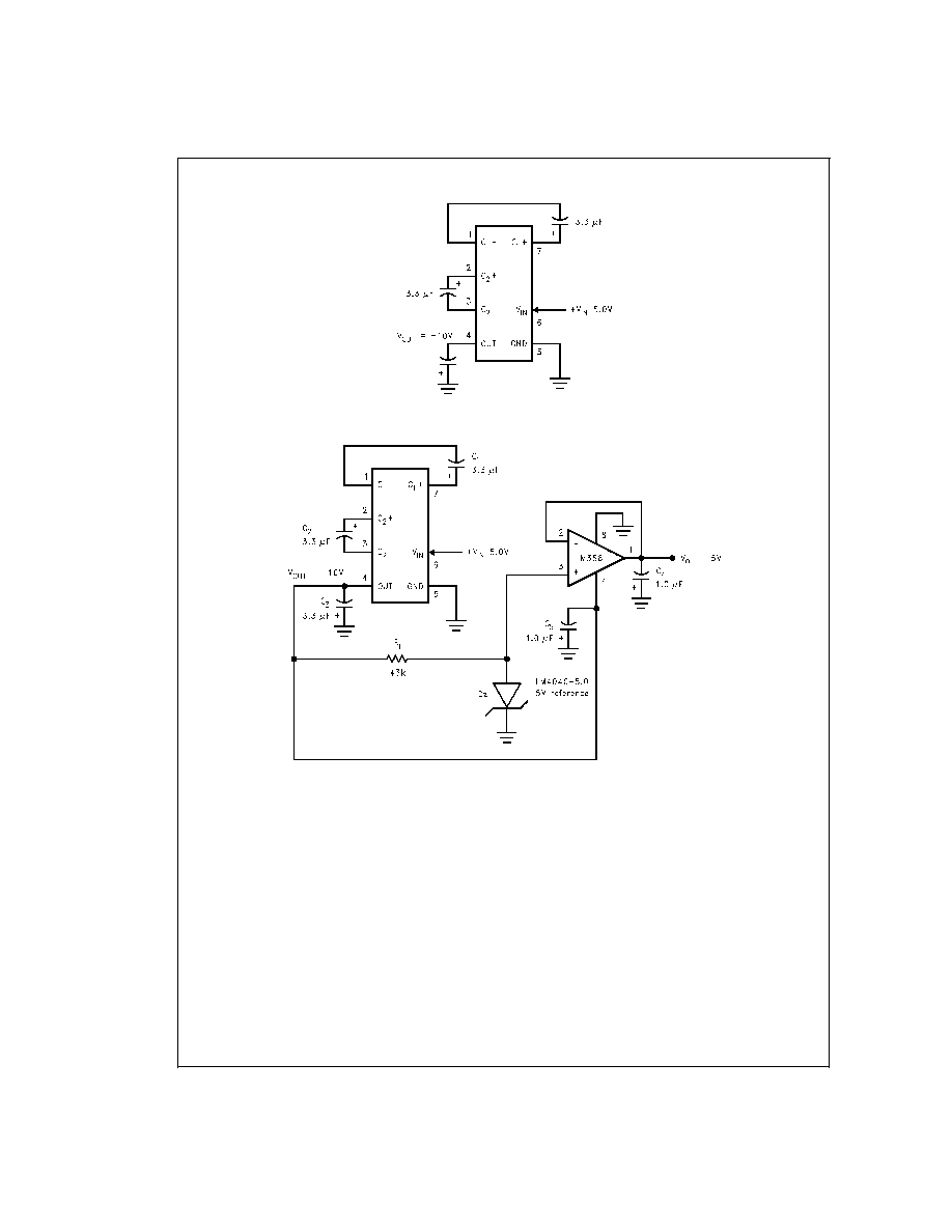
Basic Application Circuits
Application Information
Voltage Doubling Inverter
The main application of the LM2682 is to generate a nega-
tive voltage that is twice the positive input voltage. This cir-
cuit requires only three external capacitors and is connected
as shown in
Figure 1. It is important to keep in mind that the
efficiency of the circuit is determined by the output resis-
tance. A derivation of the output resistance is shown below:
R
OUT
=
2(R
SW1
+R
SW2
+ESR
C1
+R
SW3
+R
SW4
+ESR
C2
) +
2(R
SW1
+R
SW2
+ESR
C1
+R
SW3
+R
SW4
+ESR
C2
) +
1/(f
OSC
xC1) + 1/(f
OSC
xC2) + ESR
C3
Using the assumption that all four switches have the same
ON resistance our equation becomes:
R
OUT
=
16R
SW
+ 4ESR
C1
+ 4ESR
C2
+ ESR
C3
+
1/(f
OSC
xC1) + 1/(f
OSC
xC2)
Output resistance is typically 90
with an input voltage of
+5V, an operating temperature of 25∞C, and using low ESR
3.3 µF capacitors. This equation shows the importance of
capacitor selection. Large value, low ESR capacitors will re-
duce the output resistance significantly but will also require a
larger overall circuit. Smaller capacitors will take up less
space but can lower efficiency greatly if the ESR is large.
Also to be considered is that C1 must be rated at 6 VDC or
greater while C2 and C3 must be rated at 12 VDC or greater.
The amount of output voltage ripple is determined by the out-
put capacitor C3 and the output current as shown in this
equation:
V
RIPPLE P-P
= I
OUT
x (2xESR
C3
+ 1/[2x(f
OSC
xC3)])
Once again a larger capacitor with smaller ESR will give bet-
ter results.
DS100997-3
FIGURE 1. Doubling Voltage Inverter
DS100997-4
FIGURE 2. +5V to -5V Regulated Voltage Converter
LM2682
www.national.com
4

Application Information
(Continued)
+5V to -5V Regulated Voltage Converter
Another application in which the LM2682 can be used is for
generating a -5V regulated supply from a +5V unregulated
supply. This involves using an op-amp and a reference and
is connected as shown in
Figure 2. The LM358 op-amp was
chosen for its low cost and versatility and the LM4040-5.0
reference was chosen for its low bias current requirement.
Of course other combinations may be used at the designer's
discretion to fit accuracy, efficiency, and cost requirements.
With this configuration the circuit is well regulated and is still
capable of providing nearly 10 mA of output current. With a 9
mA load the circuit can typically maintain 5% regulation on
the output voltage with the input varying anywhere from 4.5V
to the maximum of 5.5V. With less load the results are even
better. Voltage ripple concerns are reduced in this case since
the ripple at the output of the LM2682 is reduced at the out-
put by the PSRR of the op-amp used.
Paralleling Devices
Any number of devices can be paralleled to reduce the out-
put resistance. As shown in
Figure 3, each device must have
its own pumping capacitors, C1 and C2, but only one shared
output capacitor is required. The effective output resistance
is the output resistance of one device divided by the number
of devices used in parallel. Paralleling devices also gives the
capability of increasing the maximum output current. The
maximum output current now becomes the maximum output
current for one device multiplied by the number of devices
used in parallel. For example, if you parallel two devices you
can get 20 mA of output current and have half the output re-
sistance of one device supplying 10 mA.
DS100997-5
FIGURE 3. Paralleling Devices
LM2682
www.national.com
5