 | –≠–ª–µ–∫—Ç—Ä–æ–Ω–Ω—ã–π –∫–æ–º–ø–æ–Ω–µ–Ω—Ç: LM2685 | –°–∫–∞—á–∞—Ç—å:  PDF PDF  ZIP ZIP |

LM2685
Dual Output Regulated Switched Capacitor Voltage
Converter
General Description
The LM2685 CMOS charge-pump voltage converter oper-
ates as an input voltage doubler, +5V regulator and inverter
for an input voltage in the range of +2.85V to +6.5V. Five low
cost capacitors are used in this circuit to provide up to 50mA
of output current at +5V (
±
5%), and 15mA at -5V. The
LM2685 operates at a 130 kHz switching frequency to re-
duce output resistance and voltage ripple. With an operating
current of only 800µA (operating efficiency greater than 80%
with most loads) and 6µA typical shutdown current, the
LM2685 is ideal for use in battery powered systems. The de-
vice is in a small 14-pin TSSOP package.
Features
n
+5V regulated output
n
Inverts V
05
(+5V) to V
NEG
(-5V)
n
Doubles input supply voltage
n
TSSOP-14 package
n
80% typical conversion efficiency at 25mA
n
Input voltage range of 2.85V to 6.5V
n
Independent shutdown control pins
Applications
n
Cellular phones
n
Pagers
n
PDAs
n
Handheld instrumentation
n
3.3V to 5V voltage conversion applications
Typical Application and Connection Diagram
Ordering Information
Order Number
Package Type
NSC Package
Drawing
Supplied As
LM2685MTC
TSSOP-14
MTC14
94 Units, Rail
LM2685MTCX
TSSOP-14
MTC14
2.5k Units, Tape and Reel
DS101100-1
DS101100-2
14-Pin TSSOP
May 2000
LM2685
Dual
Output
Regulated
Switched
Capacitor
V
oltage
Converter
© 2000 National Semiconductor Corporation
DS101100
www.national.com

Pin Description
Pin No.
Name
Function
1
V
IN
Power supply input voltage.
2
GND
Power supply ground.
3
V
NEG
Negative output voltage created by inverting V
05
.
4
V
NSW
V
NEG
output connected through a series switch, NSW.
5
CE
Chip enable input. This pin is high for normal operation and low for shutdown. (See
Shutdown and Load Disconnect section in the Detailed Device Description division).
6
SDP
Positive side shutdown input. This pin is low for normal operation and high for positive
side shutdown and V
PSW
load disconnect. (See Shutdown and Load Disconnect section
in the Detailed Device Description division).
7
SDN
Negative side shutdown input. This pin is low for normal operation and high for negative
side shutdown and V
NSW
load disconnect. (See Shutdown and Load Disconnect section
in the Detailed Device Description division).
8
C
2
-
The negative terminal of inverting charge-pump capacitor, C2.
9
C
2
+
The positive terminal of inverting charge-pump capacitor, C2.
10
V
05
Regulated +5V output.
11
V
PSW
V
05
output connected through a series switch, PSW.
12
V
DBL
Voltage Doubler Output. (2.85V
V
IN
5.4V. See Voltage Doubler section).
13
C
1
+
The positive terminal of doubling charge-pump capacitor, C1.
14
C
1
-
The negative terminal of doubling charge-pump capacitor, C1.
LM2685
www.national.com
2

Absolute Maximum Ratings
(Note 1)
If Military/Aerospace specified devices are required,
please contact the National Semiconductor Sales Office/
Distributors for availability and specifications.
Supply Voltage (V
IN
to GND or
GND to V
NEG
)
6.8V
SDN, SDP, CE
(GND - 0.3V) to
(V
IN
+ 0.3V)
V
05
Continuous Output Current
80mA
V
05
Short-Circuit Duration to GND
(Note 2)
Indefinite
Continuous Power Dissipation (T
A
= 25∞C) (Note 3)
600mW
T
JMAX
(Note 3)
150∞C
JA
(Note 3)
140∞C/W
Operating Ambient Temp. Range
-40∞C to 85∞C
Operating Junction Temp. Range
-40∞C to 125∞C
Storage Temp. Range
-65∞C to 150∞C
Lead Temp. (Soldering, 10 sec.)
300∞C
ESD Rating (Note 4)
2kV
Electrical Characteristics
Limits with standard typeface apply for T
J
= 25∞C, and limits in boldface type apply over the full temperature range. Unless
otherwise specified V
IN
= 3.6V, C
1
= C
2
= C
3
= C
5
= 2.2µF. C
4
= 4.7µF (Note 5)
Symbol
Parameter
Conditions
Min
Typ
Max
Units
V
+
Supply Voltage
2.85
6.5
V
I
Q
Supply Current
No Load
800
1600
µA
No Load, V
IN
= 6.5V
300
600
I
SD
Shutdown Supply Current
V
IN
= 6.5V
6
30
µA
V
SD
Shutdown Pin Input Voltage for
CE, SDP, SDN
Logic Input High
@
6.5V
2.4
V
Logic Input Low
@
6.5V
0.8
I
L
(+5V)
Output Current at V
05
2.85V
<
V
IN
<
6.5V
50
mA
R
O
(-5V)
Output Resistance at V
NEG
I
L
= 15mA (Note 6)
20
40
F
SW
Switch Frequency
85
130
180
kHz
P
EFF
Average Power Efficiency at V
05
2.85V
V
IN
6.5V
I
L
= 25mA to GND
82
%
V
05
Output Regulation
1mA
<
I
L
<
50mA, V
IN
= 6.5V
(Note 7)
4.848
5.05
5.252
V
1mA
<
I
L
<
50mA, V
IN
= 6.5V
(Note 7)
4.797
5.05
5.303
G
LINE
Line Regulation
2.85V
<
V
IN
<
3.6V
0.25
%/V
3.6V
<
V
IN
<
6.5V
0.05
G
LOAD
Load Regulation
1mA
<
I
L
<
50mA, V
IN
= 6.5V
0.3
1.0
%
R
SW
Series Switch Resistance V
NEG
to
V
NSW
V
IN
>
2.85V
1.5
V
05
to V
PSW
5.0
Note 1: Absolute Maximum Ratings indicate limits beyond which damage to the device may occur. Operating Ratings indicate conditions for which the device is in-
tended to be functional, but do not guarantee specific performance limits. For guaranteed specifications and test conditions, see the Electrical Characteristics.
Note 2: V
05
may be shorted to GND without damage. However, shorting V
NEG
to V
05
may damage the device and must be avoided. Also, for temperature above
85∞C, V
05
must not be shorted to GND or device may be damaged.
Note 3: The maximum allowable power dissipation is calculated by using P
DMAX
= (T
JMAX
-- T
A
)/
JA
, where T
JMAX
is the maximum junction temperature, T
A
is the
ambient temperature and
JA
is the junction-to-ambient thermal resistance of the specified package.
Note 4: The human body model is a 100 pF capacitor discharged through a 1.5k
resistor into each pin.
Note 5: In the typical operating circuit, capacitors C
1
and C
2
are 2.2µF, 0.3
maximum ESR capacitors. Capacitors with higher ESR will increase output resistance,
reduce output voltage and efficiency.
Note 6: Specified output resistance includes internal switch resistance and ESR of capacitors. See the Detailed Device Description section.
Note 7: The 50 mA maximum current assumes no current is drawn from V
DBL
pin. See Voltage Doubler section in the Detailed Device Description.
LM2685
www.national.com
3
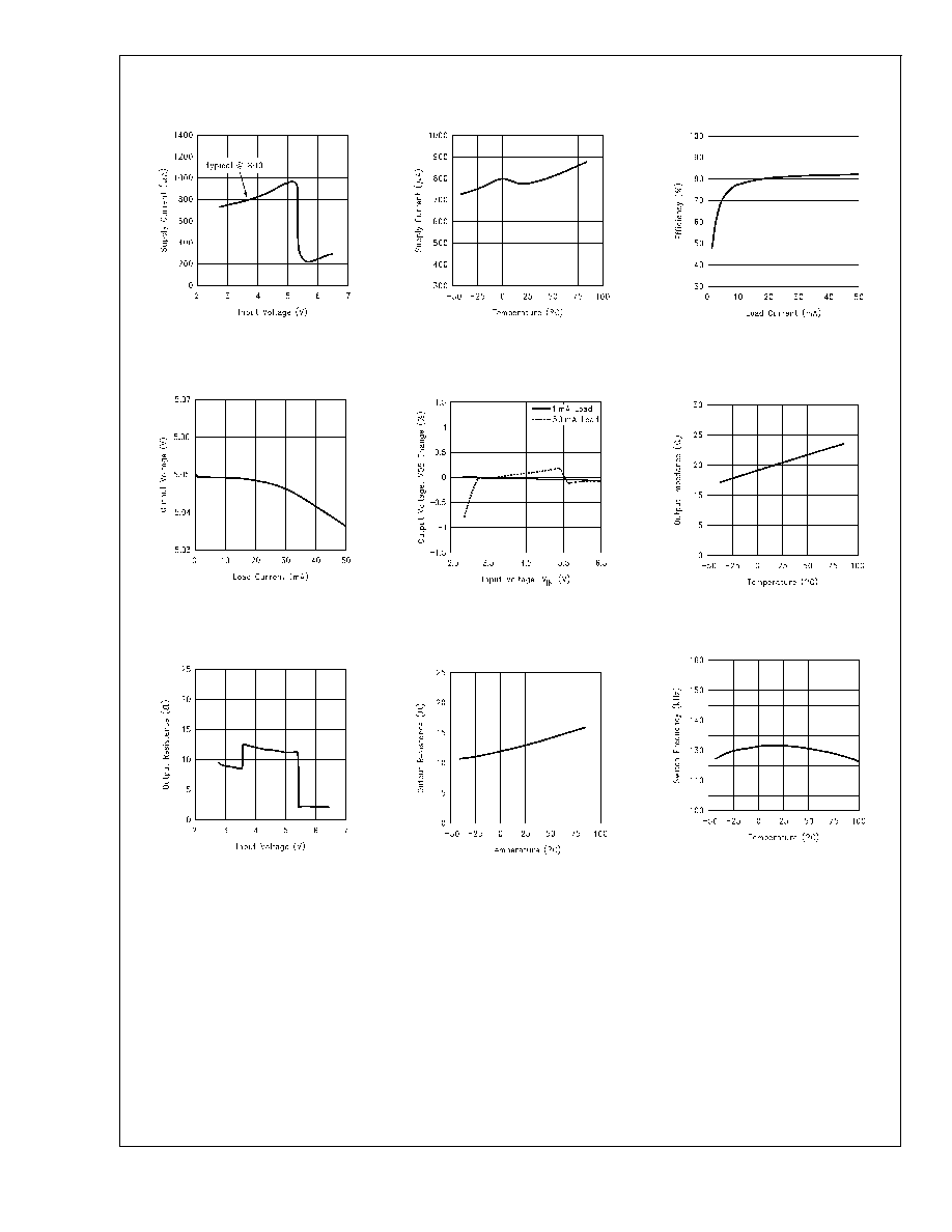
Typical Performance Characteristics
Unless otherwise specified, T
A
= 25∞C, V
IN
= 3.6V.
Supply Current vs Input Voltage
DS101100-6
Supply Current vs Temperature
DS101100-7
Efficiency vs Load Current
DS101100-8
Output Voltage (V
05
) vs.
Load Current
DS101100-9
V
05
Voltage vs.
Input Voltage
DS101100-21
Output Resistance (VNEG) vs.
Temperature
DS101100-10
Output Resistance (VDBL) vs.
Input Voltage
DS101100-11
Output Resistance (VDBL) vs.
Temperature
DS101100-12
Switch Frequency vs. Temperature
DS101100-13
LM2685
www.national.com
4

Typical Performance Characteristics
Unless otherwise specified, T
A
= 25∞C, V
IN
=
3.6V. (Continued)
Line Transient Response (with 5mA
Load)
DS101100-14
A: INPUT VOLTAGE: V
IN
= 3.2V to 6.0V, 5V/div
B: OUTPUT VOLTAGE: V
PSW
: 100mV/div
C: OUTPUT VOLTAGE: V
NSW
: 100mV/div
V
05
Load Transient Response
DS101100-15
A: LOAD CURRENT: I
LOAD
= 5mA to 39.6mA,
10mA/div
B: OUTPUT VOLTAGE: V
05
: 10mV/div
V
NSW
Load Transient Response
DS101100-16
A: LOAD CURRENT: I
LOAD
= 4.4mA to -9.4mA,
10mA/div
B: OUTPUT VOLTAGE: V
NSW
: 50mV/div
V
PSW
and V
NSW
Response to CE
(with 5mA Load)
DS101100-17
A: CE INPUT: 5V/div
B: OUTPUT VOLTAGE: V
PSW
: 5V/div
C: OUTPUT VOLTAGE: V
NSW
: 5V/div
V
05
Response to SDP (with 5mA
Load)
DS101100-18
A: SDP INPUT: 5V/div
B: OUTPUT VOLTAGE: 5V/div
V
NSW
Response to SDP (with 5mA
Load)
DS101100-19
A: SDP INPUT: 5V/div
B: OUTPUT VOLTAGE (V
NSW
): 5V/div
V
NSW
Response to SDN
(with 5mA Load)
DS101100-20
A: SDN INPUT: 5V/div
B: OUTPUT VOLTAGE (V
NSW
): 5V/div
LM2685
www.national.com
5