LM2715
TFT Panel Module
General Description
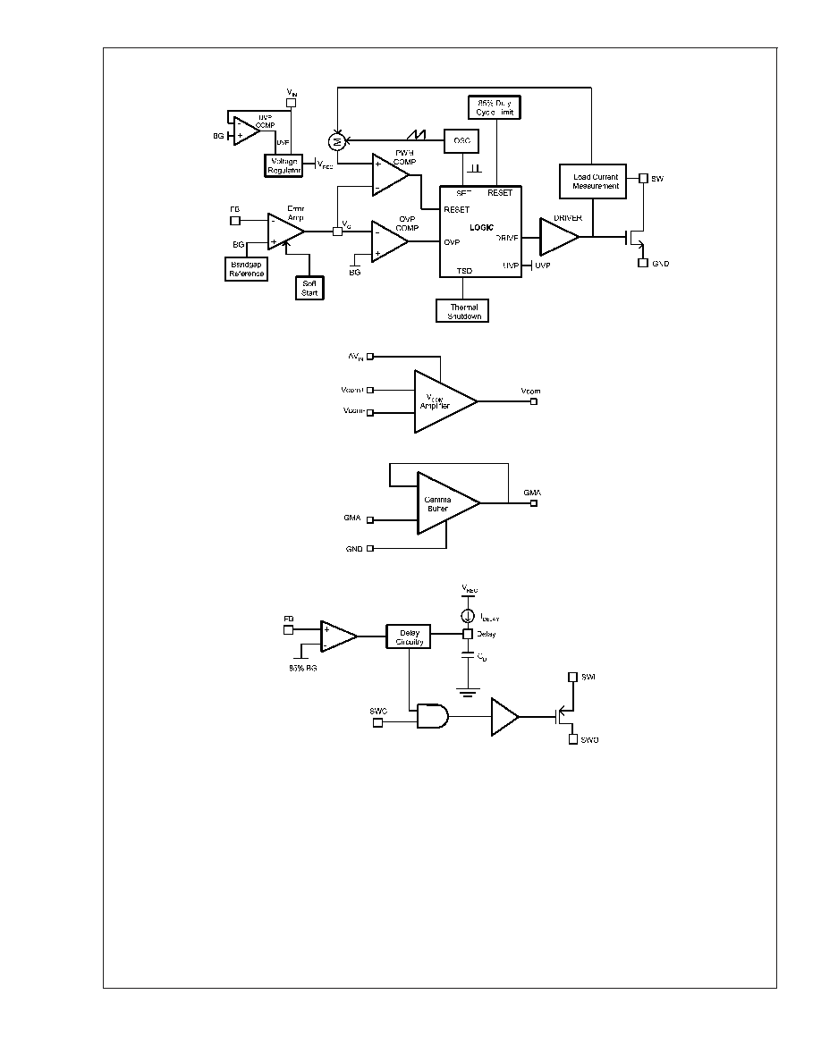
The LM2715 is a compact bias solution for TFT displays. It
has a current mode PWM step-up DC/DC converter with a
1.3A, 0.18
internal switch. Capable of generating 8V at
240mA from a Lithium Ion battery, the LM2715 is ideal for
generating bias voltages for large screen LCD panels. The
LM2715 operates at a switching frequency of 1.25MHz al-
lowing for easy filtering and low noise. An external compen-
sation pin gives the user flexibility in setting frequency com-
pensation, which makes possible the use of small, low ESR
ceramic capacitors at the output. The LM2715 uses a pat-
ented internal circuitry to limit startup inrush current of the
boost switching regulator without the use of an external
softstart capacitor. The LM2715 has an internal controllable
PMOS switch used for controlling the row driver voltages.
The switch can be controlled externally with a control pin and
delay time. The LM2715 contains a Vcom amplifier and a
Gamma buffer capable of supplying 50mA source and sink.
The TSSOP-16 package ensures a low profile overall solu-
tion.
Features
n
1.3A, 0.18
, internal power switch
n
V
IN
operating range: 2.2V to 12V
n
1.25MHz switching frequency step-up DC/DC converter
n
Inrush current limiting circuitry
n
Internal 7
PMOS switch
n
PMOS switch control pin
n
PMOS switch delay pin
n
Vcom amplifier
n
Gamma buffer
n
16 pin TSSOP package
Applications
n
LCD Bias Supplies
Typical Application Circuit
20058431
May 2003
LM2715
TFT
Panel
Module
© 2003 National Semiconductor Corporation
DS200584
www.national.com
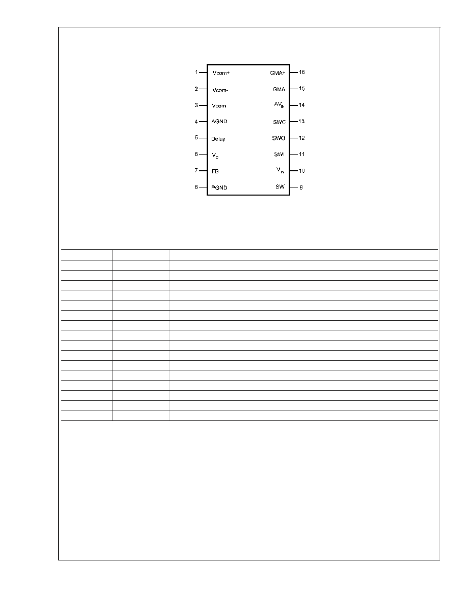
Connection Diagram
Top View
20058404
TSSOP 16 package
T
JMAX
= 125∞C,
JA
= 120∞C/W (Note 1)
Pin Description
Pin
Name
Function
1
Vcom+
Vcom Amplifier positive input.
2
Vcom-
Vcom Amplifier negative input.
3
Vcom
Vcom Amplifier output.
4
AGND
Analog Ground. Connect to AGND plane.
5
Delay
PMOS switch delay.
6
V
C
Boost Compensation Network Connection.
7
FB
Output Voltage Feedback input.
8
PGND
Power Ground. Connect to PGND plane.
9
SW
NMOS power switch input.
10
V
IN
Main power input, step-up and switch circuitry.
11
SWI
PMOS switch input.
12
SWO
PMOS switch output.
13
SWC
PMOS switch control pin.
14
AV
IN
Analog power input (buffers).
15
GMA
Gamma buffer output.
16
GMA+
Gamma buffer input.
LM2715
www.national.com
2

Pin Functions
Vcom+(Pin 1): Positive input terminal of Vcom amplifier.
Vcom-(Pin 2): Negative input terminal of Vcom amplifier.
Vcom(Pin 3): Output terminal of Vcom amplifier.
AGND(Pin 4): Analog ground connection for LM2715. Con-
nect all sensitive circuitry, ie. feedback resistors, delay ca-
pacitor, and compensation network to its own dedicated
AGND plane which connects directly to this pin.
Delay(Pin 5): PMOS switch delay control pin. See Operation
section for setting the delay time.
The delay time begins when the output voltage of the DC/DC
switching regulator reaches 85% of its true output voltage.
This corresponds to a FB voltage of about 1.1V. The PMOS
switch is controlled with both the delay time and the switch
control pin, SWC. If no Cdelay capacitor is used, the PMOS
switch is controlled solely with the SWC pin.
V
C
(Pin 6): Compensation Network for Boost switching regu-
lator. Connect resistor/capacitor network between V
C
pin
and AGND for boost switching regulator AC compensation.
FB(Pin 7): Feedback pin. Set the output voltage by selecting
values of R1 and R2 using:
Connect the ground of the feedback network to the AGND
plane, which should be tied directly to the PGND pin.
PGND(Pin 8):Connect all power ground components to a
PGND plane which should also connect directly to this pin.
Use a trace or via to connect the AGND plane to the PGND
plane. Please see Layout Considerations under the Opera-
tion section for more details on layout suggestions.
SW(Pin 9): This is the drain of the internal NMOS power
switch. Minimize the metal trace area connected to this pin to
minimize EMI.
V
IN
(Pin 10): Input Supply Pin. Bypass this pin with a capaci-
tor as close to the device as possible. The capacitor should
connect between V
IN
and PGND.
SWI(Pin 11): PMOS switch input. Source connection of
PMOS device.
SWO(Pin 12): PMOS switch output. Drain connection of
PMOS device.
SWC(Pin13): PMOS switch control pin. This pin creates an
AND function with the delay time after the output of the
switching regulator has reached 85% of its nominal value. To
ensure the PMOS switch is in the correct state, apply a
voltage above 1.5V to this pin to turn on the PMOS switch
and apply a voltage below 0.7V to turn off the PMOS switch.
AV
IN
(Pin 14): Supply pin for the Vcom opamp and the
Gamma buffer. Bypass this pin with a capacitor as close to
the device as possible, about 100nF, if connected directly to
the output of the boost DC/DC switching regulator. The
capacitor should connect between AV
IN
and PGND.
GMA(Pin 15): Gamma Buffer output pin.
GMA+(Pin 16): Gamma Buffer input pin.
Ordering Information
Order Number
Package Type
NSC Package Drawing
Supplied As
LM2715MT-ADJ
TSSOP-16
MTC16
73 Units, Rail
LM2715MTX-ADJ
TSSOP-16
MTC16
2500 Units, Tape and Reel
LM2715
www.national.com
3
Absolute Maximum Ratings
(Note 2)
If Military/Aerospace specified devices are required,
please contact the National Semiconductor Sales Office/
Distributors for availability and specifications.
V
IN
-0.3V to 12V
SW Voltage
-0.3V to 18V
FB Voltage
-0.3V to 2V
V
C
Voltage
0.96V to 1.56V
SWC Voltage
-0.3V to 12V
Supply Voltage, AV
IN
-0.3V to 12V
Amplifier/Buffer Input Voltage
Rail-to-Rail
Amplifier/Buffer Output
Voltage
Rail-to-Rail
Delay
GND to 1.3V
SWI
-0.3V to 30V
SWO
-0.3V to 30V
ESD Ratings
(Note 3)
Human Body Model
2kV
Machine Model
200V
Operating Conditions
Operating Temperature
-40∞C to +125∞C
Storage Temperature
-65∞C to +150∞C
Supply Voltage, V
IN
2.2V to 12V
SW Voltage
17.5V
Supply AV
IN
4V to 12V
SWI
2.2V to 30V
Electrical Characteristics
Specifications in standard type face are for T
J
= 25∞C and those with boldface type apply over the full Operating Tempera-
ture Range ( T
J
= -40∞C to +125∞C). Unless otherwise specified V
IN
=2.2V, AV
IN
= 8V, R
COM
= R
GAMMA
= 50
, C
COM
=
C
GAMMA
= 1nF.
Switching Regulator
Symbol
Parameter
Conditions
Min
(Note 4)
Typ
(Note 5)
Max
(Note 4)
Units
I
Q
Quiescent Current
Not Switching, FB = 2V
1.6
2.3
mA
Switching, switch open, FB =
0.1V
3.6
4.3
V
FB
Feedback Voltage
1.239
1.265
1.291
V
%V
FB
/
V
IN
Feedback Voltage Line
Regulation
0.01
0.1
%/V
I
CL
Switch Current Limit
(Note 6)
V
IN
= 2.5V, V
OUT
= 8V
1.29
A
R
DSON
Switch R
DSON
(Note 7)
V
IN
= 2.5V
178
m
I
B
FB Pin Bias Current (Note 8)
60
200
nA
V
IN
Input Voltage Range
2.2
12
V
T
SS
Internal Soft Start Ramp
Time
7
mS
g
m
Error Amp Transconductance
I = 5µA
85
110
270
µmho
A
V
Error Amp Voltage Gain
135
V/V
D
MAX
Maximum Duty Cycle
78
85
%
f
S
Switching Frequency
1.0
1.25
1.5
MHz
I
L
Switch Leakage Current
V
SW
= 18V
0.1
20
µA
UVP
On Threshold
1.79
1.92
2.05
V
Off Threshold
1.69
1.82
1.95
V
Hysteresis
100
mV
LM2715
www.national.com
5