 | –≠–ª–µ–∫—Ç—Ä–æ–Ω–Ω—ã–π –∫–æ–º–ø–æ–Ω–µ–Ω—Ç: LM2753SD | –°–∫–∞—á–∞—Ç—å:  PDF PDF  ZIP ZIP |

LM2753
High Power Switched Capacitor Voltage Convertor/Flash
LED Driver
General Description
The LM2753 is capable of driving a Flash LED with a pulsed
current of 400mA at an input voltage of 3.6V. A switched
capacitor doubler, the LM2753 provides a regulated 5V out-
put (V
OUT
) over an input supply range of 3.0V to 5.5V. The
switched output, I
OUT
, takes less than 10ns to turn on and
provide maximum current to a Flash LED. Flash LED current
is set via a ballast resistor. Continuous illumination current
(Torch Mode) is programmed by connecting a resistor be-
tween I
OUT
and V
OUT
. This device uses only three small,
low-cost ceramic capacitors.
LM2753 uses Pulse Frequency Modulation (PFM) regula-
tion. Typical operating frequency is 725kHz. Under no-load
conditions, LM2753 operates on only 60µA. If the output is
connected to ground, the charge pump stays in the gain of 1
which helps limit the input current to 300mA (typ.)
LM2753 is available in a 10-pin No Pullback Leadless Lead-
frame Package: LLP-10.
Features
n
Input Voltage Range: 3.0V to 5.5V
n
Regulated 5V Output
n
250mA Output Current with a 3.6V input
n
400mA Pulsed Output Current (up to 500ms duration)
n
60µA (typ.) Quiescent Current
n
PFM Regulation
n
Inductor-less solution: requires only 3 small capacitors
n
<
1µA Typical Shutdown Current
n
10-pin LLP Package (No Pullback):
3mm x 3mm x 0.75mm
Applications
n
Cell Phone Camera Flash
n
General Purpose Regulated Voltage Output, High
Current Supply
Typical Application Circuit
20140601
February 2005
LM2753
High
Power
Switched
Capacitor
V
oltage
Convertor/Flash
LED
Driver
© 2005 National Semiconductor Corporation
DS201406
www.national.com
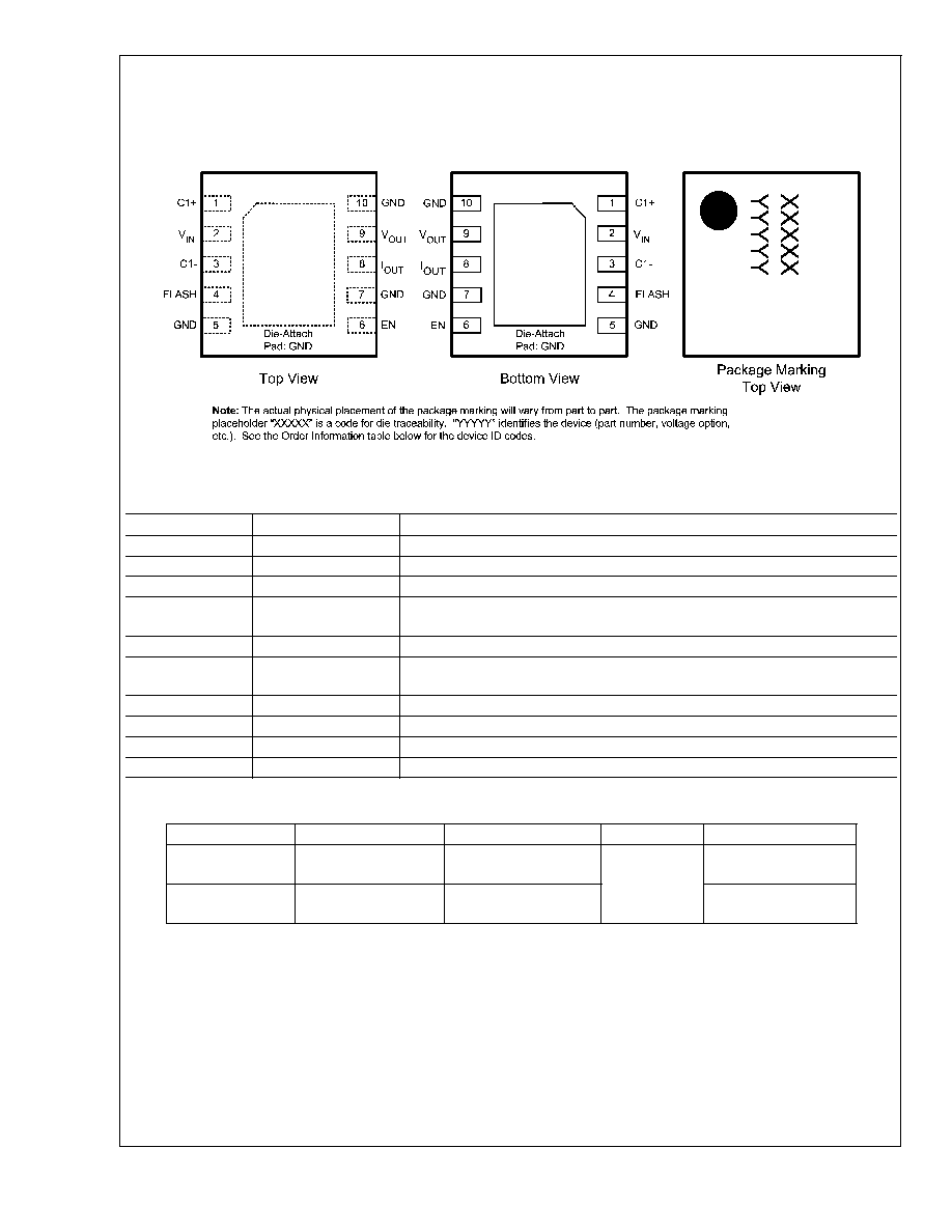
Connection Diagram
LM2753
10-Pin LLPPackage (LLP10) No Pullback
3mm X 3mm x 0.75mm
NS Package Number SDA10A
20140605
Pin Descriptions
Pin #
Name
Description
1
C
1+
Flying capacitor connection.
2
V
IN
Input Voltage Connection. Input Voltage Range: 3.0V to 5.5V.
3
C
1-
Flying Capacitor connection.
4
FLASH
Flash Logic Input Pin. Logic HIGH = Flash Output On, Logic LOW = Flash
Output Off. There is an internal pulldown of 300k
between FLASH and GND.
5
GND
Connect to Ground.
6
EN
Enable Pin. Logic HIGH = Enable, Logic LOW = Shut Down. There is an
internal pulldown of 300k
between EN and GND
7
GND
Connect to Ground.
8
I
OUT
Flash Output. On/Off Control via FLASH Pin.
9
V
OUT
5V Regulated Output.
10
GND
Connect to Ground
Ordering Information
Output Voltage
Ordering Number
Package Mark ID
Package
Supplied As
5.0V
LM2753SD
D004B
SDA10A
Non-Pullback
LLP
250 Units, Tape and
Reel
5.0V
LM2753SDX
D004B
3000 Units, Tape and
Reel
LM2753
www.national.com
2

Absolute Maximum Ratings
(Notes 1, 2)
If Military/Aerospace specified devices are required,
please contact the National Semiconductor Sales Office/
Distributors for availability and specifications. If Military/
Aerospace specified devices are required, please contact
the National semiconductor Sales/Office/Distributors for
availability and specifications.
V
IN
Pin: Voltage to Ground
-0.3V to 6.0V
EN, Flash pins: Voltage to GND
-0.3V to (V
IN
+0.3)
w/ 6.0V max
Continuous Power Dissipation (Note
3)
Internally Limited
Junction Temperature (T
J-MAX-ABS
)
150∞C
Storage Temperature Range
-65∞C to 150∞C
Maximum Lead Temperature
265∞C
(Soldering, 10sec.)
ESD Rating (Note 4)
Human-body model:
Machine model:
2kV
200V
Operating Ratings
(Notes 1, 2)
Input Voltage Range
3.0V to 5.5V
EN, Flash Input Voltage Range
0V to V
IN
Junction Temperature (T
J
) Range
-40∞C to 120∞C
Ambient Temperature (T
A
) Range
-40∞C to 85∞C
(Note 5)
Thermal Properties
Junction-to-Ambient Thermal
Resistance, LLP-10
55∞C/W
Package (
JA
) (Note 6)
Electrical Characteristics
(Notes 2, 7)
Limits in standard typeface are for T
A
= 25
o
C. Limits in boldface type apply over the full operating ambient temperature range
(-40∞C
T
A
+85∞C) . Unless otherwise noted, specifications apply to the LM2753 Typical Application Circuit (pg. 1) with: V
IN
= 3.6V, V(EN) = V
IN,
V(FLASH) = GND, C
1
= 1.0µF, C
IN
= C
OUT
= 10.0µF (Note 8).
Symbol
Parameter
Conditions
Min
Typ
Max
Units
V
OUT
Output Voltage
3.0V
V
IN
5.5V,
I
OUT
100mA
4.75
(-5%)
5.0
5.25
(+5%)
V
I
VOUT
Continuous Load Current
3.0V
V
IN
5.5V
V
OUT
= 5V (typ.)
200
mA
I
OUT
Pulsed Flash Current
V(FLASH) = 1.8V
T
PULSE
= 500mS
V
IOUT-MAX
= 4.1V (typ.)
400
mA
I
Q
Quiescent Current
I
OUT
= 0mA
3.0V
V
IN
5.5V
60
80
µA
I
SD
Shutdown Supply Current
V(EN) = 0V
3.0V
V
IN
5.5V
0.1
1
µA
V(EN) = 0V
3.0V
V
IN
5.5V
TA = 85∞C
0.2
R
OUT
Output Impedance
V
IN
= 3.2V
5.3
fsw
Switching Frequency
3.0V
V
IN
5.5V
475
725
950
kHz
V
IH
Logic Input High
Input Pins: EN, FLASH
1.20
V
IN
V
V
IL
Logic Input Low
Input Pins: EN, FLASH
0
.30
V
I
IH
Logic Input High Current
V(EN) = V(FLASH) = 3.0V
10
µA
I
IL
Logic Input Low Current
V(EN) = V(FLASH) = 0V
10
nA
t
ON
Turn-On Time (Note 9)
640
µs
t
FLASH
Flash Turn-On Time (Note 10)
V(FLASH) = 3.6V
10
ns
Note 1: Absolute Maximum Ratings indicate limits beyond which damage to the component may occur. Operating Ratings are conditions under which operation of
the device is guaranteed. Operating Ratings do not imply guaranteed performance limits. For guaranteed performance limits and associated test conditions, see the
Electrical Characteristics tables.
Note 2: All voltages are with respect to the potential at the GND pin.
Note 3: Internal thermal shutdown circuitry protects the device from permanent damage. Thermal shutdown engages at T
J
=125∞C (typ.).
Note 4: The Human body model is a 100 pF capacitor discharged through a 1.5 k
resistor into each pin. The machine model is a 200pF capacitor discharged
directly into each pin. MIL-STD-883 3015.7
LM2753
www.national.com
3

Electrical Characteristics
(Notes 2, 7) (Continued)
Note 5: In applications where high power dissipation and/or poor package thermal resistance is present, the maximum ambient temperature may have to be
derated. Maximum ambient temperature (T
A-MAX
) is dependent on the maximum operationg junction temperature (T
J-MAX-OP
= 120
o
C), the maximum power
dissipation of the device in the application (P
D-MAX
), and the junction-to ambient thermal resistance of the part/package in the application (
JA
), as given by the
following equation: T
A-MAX
= T
J-MAX-OP
- (
JA
x P
D-MAX
).
Note 6: Junction-to-ambient thermal resistance (
JA
) is taken from a thermal modeling result, performed under the conditions and guidelines set forth in the JEDEC
standard JESD51-7. The test board is a 4 layer FR-4 board measuring 102mm x 76mm x 1.6mm with a 2 x 1 array of thermal vias. The ground plane on the board
is 50mm x 50mm. Thickness of copper layers are 36µm/18µm /18µm/36µm (1.5oz/1oz/1oz/1.5oz). Ambient temperature in simulation is 22∞C, still air. Power
dissipation is 1W.
The value of
JA
of the LM2753 in LLP-10 could fall in a range as wide as 50
o
C/W to 150
o
C/W (if not wider), depending on PWB material, layout, and environmental
conditions. In applications where high maximum power dissipation exists (high V
IN
, high I
OUT
), special care must be paid to thermal dissipation issues. For more
information on these topics, please refer to Application Note 1187: Leadless Leadframe Package (LLP) and the Power Efficiency and Power Dissipation
section of this datasheet..
Note 7: Min and Max limits are guaranteed by design, test, or statistical analysis. Typical numbers are not guaranteed, but do represent the most likely norm.
Note 8: C
IN
, C
OUT
, and C
1
: Low-ESR Surface-Mount Ceramic Capacitors (MLCCs) used in setting electrical characteristics
Note 9: Turn-on time is measured from when the EN signal is pulled high until the output voltage on V
OUT
crosses 90% of its final value.
Note 10: Flash Turn-on time is measured from when the FLASH signal is pulled high until the voltage on I
OUT
crosses 90% of its final programmed value.
Block Diagram
20140606
LM2753
www.national.com
4

Application Information
CIRCUIT DESCRIPTION
The LM2753 is a Switched Capacitor Doubler with a regu-
lated 5V output. It is capable of continuously supplying up to
200mA at 5V to a load connected to V
OUT
. This device uses
Pulse Frequency Modulation and a Multi-Level Switch Array
to regulate and maintain the output voltage. For higher load
currents, such as during Flash operation, the output voltage
is allowed to droop to supply the necessary current. Although
there is no current limit on this device, the device will auto-
matically default to a gain of 1 when the output is brought
below the input voltage. This configuration limits the input
current to about 300mA (typ.). The operating range for the
LM2753 is over the extended Li-Ion battery range from 2.7V
to 5.5V.
Aside from powering Flash LEDs, the LM2753 is suitable for
driving other devices with power requirements up to 200mA.
White LEDs can also be connected to this device to backlight
a cellular phone keypad and display. The LED brightness
can be controlled by applying a PWM (Pulse Width Modula-
tion) signal to the Enable pin (EN) during "Torch" mode, or to
the Flash pin during "Flash" mode. (see PWM BRIGHT-
NESS CONTROL PROCEDURES section).
SOFT START
Soft Start is engaged when the device is taken out of Shut-
down mode (EN = logic HIGH) or when voltage is supplied
simultaneously to the VIN and EN pins. During Soft Start, the
voltage on V
OUT
will ramp up in proportion to the rate that the
reference voltage is being ramped up. The output voltage is
programmed to rise from 0V to 5V in 640µs (typ.).
ENABLE MODE
The Enable logic pin (EN) disables the part and reduces the
quiescent current to 0.1µA (typ.). The LM2753 has an active-
high enable pin (LOW = shut down, HIGH = operating). The
LM2753 EN pin can be driven with a low-voltage CMOS logic
signal (1.5V logic, 1.8V logic, etc). There is an internal
300k
pull-down resistor between the EN and GND pins of
the LM2753.
FLASH MODE
The Flash logic pin (Flash) controls the internal FET con-
nected between the V
OUT
and I
OUT
pins on the LM2753. The
LM2753 has an active-HIGH Flash pin (LOW = shut down,
HIGH = operating). A logic HIGH signal must be present on
the EN pin before a logic HIGH signal is place on the Flash
input pin. The EN and Flash input pins can be connected
together and controlled with the same logic signal. The
turn-on time for I
OUT
in this configuration will be limited by
the turn-on time of the device. The turn-on time for the
internal FET is typically 10ns when the device is already on
(EN signal HIGH, V
OUT
at 5V). The LM2753 Flash pin can be
driven with a low-voltage CMOS logic signal (1.5V logic,
1.8V logic, etc). There is an internal 300k
pull-down resis-
tor between the Flash and GND pins of the LM2753.
CAPACITOR SELECTION
The LM2753 requires 3 external capacitors for proper opera-
tion. Surface-mount multi-layer ceramic capacitors are rec-
ommended. These capacitors are small, inexpensive and
have very low equivalent series resistance (ESR,
15m
typ.). Tantalum capacitors, OS-CON capacitors, and alumi-
num electrolytic capacitors are generally not recommended
for use with the LM2753 due to their high ESR, as compared
to ceramic capacitors.
For most applications, ceramic capacitors with X7R or X5R
temperature characteristic are preferred for use with the
LM2753. These capacitors have tight capacitance tolerance
(as good as
±
10%), hold their value over temperature (X7R:
±
15% over -55∞C to 125∞C; X5R:
±
15% over -55∞C to
85∞C), and typically have little voltage coefficient when com-
pared to other types of capacitors. However selecting a
capacitor with a voltage rating much higher than the voltage
it will be subjected to, will ensure that the capacitance will
stay closer to the capacitor's nominal value. Capacitors with
Y5V or Z5U temperature characteristic are generally not
recommended for use with the LM2753. Capacitors with
these temperature characteristics typically have wide ca-
pacitance tolerance (+80%, -20%), vary significantly over
temperature (Y5V: +22%, -82% over -30∞C to +85∞C range;
Z5U: +22%, -56% over +10∞C to +85∞C range), and have
poor voltage coefficients. Under some conditions, a nominal
1µF Y5V or Z5U capacitor could have a capacitance of only
0.1µF. Such detrimental deviation is likely to cause Y5V and
Z5U capacitors to fail to meet the minimum capacitance
requirements of the LM2753. Table 1 lists suggested capaci-
tor suppliers for the typical application circuit.
TABLE 1. Ceramic Capacitor Manufacturers
Manufacturer
Contact
TDK
www.component.tdk.com
Murata
www.murata.com
Taiyo Yuden
www.t-yuden.com
FLASH LED SELECTION
The LM2753 provides a 5V (typ.) fixed voltage to drive a
Flash LED with a continuous current up to 200mA (typ.). At
LED currents above 200mA (typ.), the output of the LM2753
is allowed to droop to deliver the desired current to the Flash
LED. This droop limits the maximum forward voltage and in
turn the maximum current that can be supplied to a given
LED. LEDs should be chosen such that the LED forward
voltage at the desired maximum LED current does not ex-
ceed the output voltage of the LM2753 when loaded down
with that same current. It is suggested that the selected
LEDs be binned due to the relatively high forward voltage
tolerance of Flash LEDs. The typical and maximum diode
forward voltage depends highly on the manufacturer and
their technology. Table 2 lists several suggested manufac-
turers.
TABLE 2. Flash LED Selection
Manufacturer
Contact
Agilent
www.agilent.com/semiconductors
AOT
www.aot.com.tw
Citizen
www.c-e.co.jp/e/
Lumiled
www.lumileds.com
Nichia
www.nichia.com
Osram
www.osram-os.com
Panasonic
www.panasonic.co.jp/semicon/
Seoul Semiconductor
en.seoulsemicon.co.kr
LM2753
www.national.com
5