Äîêóìåíòàöèÿ è îïèñàíèÿ www.docs.chipfind.ru
LM2770
High Efficiency Switched Capacitor Step-Down DC/DC
Regulator with Sleep Mode
General Description
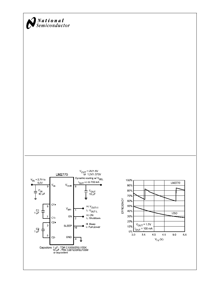
The LM2770 is a switched capacitor step-down regulator
that is ideal for powering low-voltage applications in portable
systems. The LM2770 can supply load currents up to 250mA
and operates over an input voltage range of 2.7V to 5.5V.
This makes the LM2770 a great choice for systems powered
by 1-cell Li-Ion batteries and chargers. The output voltage of
the LM2770 can be dynamically switched between two out-
put levels with a logic input pin. Output voltage pairs cur-
rently available include 1.2V/1.5V and 1.2V/1.575V. Other
pairs of voltage options can be developed upon request.
LM2770 efficiency is superior to both fixed-gain switched
capacitor buck regulators and low-dropout linear regulators
(LDO's). Multiple fractional gains maximize power efficiency
over the entire input voltage and output current ranges. The
LM2770 can also be switched into a low-power sleep mode
when load currents are light (
20mA). In sleep mode, the
charge pump is off, and the output is driven with a low-noise,
low-power linear regulator.
Soft-start, short-circuit protection, current-limit protection,
and thermal-shutdown protection are also included. The
LM2770 is available in National's small 10-pin Leadless
Leadframe Package (LLP-10).
Features
n
High Efficiency Multi-Gain Architecture: Peak Power
Efficiency
>
85%
n
Output Voltage Pairs: 1.2V/1.5V and 1.2V/1.575V
n
Dynamic Output Voltage Selection
n
±
3% Output Voltage Accuracy
n
Output Currents up to 250mA
n
2.7V to 5.5V Input Range
n
Low-Supply-Current Sleep Mode
n
55µA Quiescent Supply Current in Full-Power Mode
n
Soft-Start
n
Short-Circuit Protection in Full-Power Mode
n
Current-Limit Protection in Sleep Mode
n
LLP-10 Package (3mm x 3mm x 0.8mm)
Applications
n
DSP Power Supplies
n
Baseband Power Supplies
n
Mobile Phones and Pagers
n
Portable Electronic Equipment
Typical Application Circuit
20126001
LM2770 Efficiency vs.
Low-Dropout Linear Regulator (LDO) Efficiency
20126011
December 2004
LM2770
High
Efficiency
Switched
Capacitor
Step-Down
DC/DC
Regulator
with
Sleep
Mode
© 2004 National Semiconductor Corporation
DS201260
www.national.com
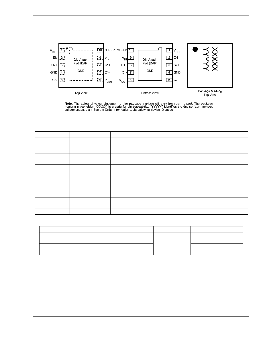
Connection Diagram and Package Mark Information
10-Pin Non-Pullback Leadless Frame Package (LLP-10)
National Semiconductor Package Number SDA10A
20126002
Pin Description
Pin #
Name
Description
1
V
SEL
Output Voltage Select Logic Input. If V
SEL
is high, V
OUT
= high voltage. If V
SEL
is low, V
OUT
= low voltage. (See Order Information for available voltage
options)
2
EN
Enable Pin Logic Input. If high, part is enabled. If low, part is in shutdown.
3
C2+
Flying Capacitor 2: Positive Termial
4
GND
Ground
5
C2-
Flying Capacitor 2: Negative terminal
10
SLEEP
Sleep Mode Logic Input. If high, the part operates in sleep mode, and the
output is driven by a low power linear regulator. If low, the part operates in
full-power mode, and the output is driven by the switched capacitor regulator
9
V
IN
Input Voltage. Recommended V
IN
operating range: 2.7V to 5.5V
8
C1+
Flying Capacitor 1: Positive Terminal
7
C1-
Flying Capacitor 1: Negative Terminal
6
V
OUT
Output Voltage
Order Information
Output Voltages
Order Number
Package Mark ID
Package
Supplied as:
1.2V / 1.5V
LM2770SD-1215
L162B
SDA10A
Non-Pullback LLP
1000 Units, Tape and Reel
1.2V / 1.5V
LM2770SDX-1215
L162B
4500 Units, Tape and Reel
1.2V / 1.575V
LM2770SD-12157
L166B
1000 Units, Tape and Reel
1.2V / 1.575V
LM2770SDX-12157
L166B
4500 Units, Tape and Reel
LM2770
www.national.com
2
Absolute Maximum Ratings
(Notes 1, 2)
If Military/Aerospace specified devices are required,
please contact the National Semiconductor Sales Office/
Distributors for availability and specifications.
V
IN
Pin Voltage
-0.3V to 6.0V
EN, SLEEP, and V
SEL
Pin Voltages
-0.3V to (V
IN
+0.3V)
w/ 6.0V max
Continuous Power Dissipation
(Note 3)
Internally Limited
V
OUT
Short to GND Duration
(Note 4)
Infinite
Junction Temperature (T
J-MAX
)
150
o
C
Storage Temperature Range
-65
o
C to +150
o
C
Maximum Lead Temperature
(Note 5)
265
o
C
ESD Rating (Note 6)
Human Body Model:
Machine Model
2.0kV
200V
Operating Ratings
(Notes 1, 2)
Input Voltage Range
2.7V to 5.5V
Recommended Load Current Range
0mA to 250mA
Junction Temperature (T
J
) Range
-30°C to +105°C
Ambient Temperature (T
A
) Range
(Note 6)
-30°C to +85°C
Thermal Properties
Juntion-to-Ambient Thermal
Resistance (
JA
), LLP10 Package
(Note 7)
55°C/W
Electrical Characteristics
(Notes 2, 9)
Limits in standard typeface are for T
J
= 25
o
C. Limits in boldface type apply over the full operating junction temperature range
(-30°C
T
J
+105°C) . Unless otherwise noted, specifications apply to the LM2770 Typical Application Circuit (pg. 1) with: V
IN
= 3.6V; V(EN) = V
SEL
= 1.8V, V(SLEEP) = 0V, C
IN
= C
OUT
= 10µF, C
1
= C
2
= 1.0µF. (Note 10)
Symbol
Parameter
Condition
Min
Typ
Max
Units
Output Voltage Specifications: Specific to Individual LM2770 Options
V
OUT-1215
LM2770-1215:
1.5V Output Voltage Regulation
V
IN
= 3.5V, I
OUT
= 150mA,
V
SEL
= 1.8V
1.443
1.495
1.547
V
3.0V
V
IN
4.5V
I
OUT
= 150mA, V
SEL
= 1.8V
1.420
1.495
1.570
4.5V
<
V
IN
5.5V,
I
OUT
= 150mA, V
SEL
= 1.8V
1.428
1.495
1.562
LM2770-1215:
1.2V Output Voltage Regulation
V
IN
= 3.5V, I
OUT
= 150mA,
V
SEL
= 0V
1.157
1.205
1.253
3.0V
V
IN
4.5V
I
OUT
- 150mA, V
SEL
=0V
1.140
1.205
1.270
4.5V
<
V
IN
5.5V,
I
OUT
= 150mA, V
SEL
= 0V
1.135
1.205
1.275
V
OUT-12157
LM2770-12157:
1.575V Output Voltage
Regulation
V
IN
= 3.5V, I
OUT
= 150mA,
V
SEL
= 1.8V
1.528
1.575
1.622
V
3.1V
V
IN
4.5V
I
OUT
= 150mA, V
SEL
= 1.8V
1.500
1.575
1.650
4.5V
<
V
IN
5.5V,
I
OUT
= 150mA, V
SEL
= 1.8V
1.504
1.575
1.646
LM2770-12157:
1.2V Output Voltage Regulation
V
IN
= 3.5V, I
OUT
= 150mA,
V
SEL
= 0V
1.162
1.210
1.258
3.0V
V
IN
4.5V
I
OUT
- 150mA, V
SEL
=0V
1.145
1.210
1.275
4.5V
<
V
IN
5.5V,
I
OUT
= 150mA, V
SEL
= 0V
1.145
1.210
1.275
V
OUT
/I
OUT
Load Regulation
I
OUT
= 1mA to 250mA
0.18
mV/mA
LM2770
www.national.com
3
Electrical Characteristics
(Notes 2, 9) (Continued)
Limits in standard typeface are for T
J
= 25
o
C. Limits in boldface type apply over the full operating junction temperature range
(-30°C
T
J
+105°C) . Unless otherwise noted, specifications apply to the LM2770 Typical Application Circuit (pg. 1) with: V
IN
= 3.6V; V(EN) = V
SEL
= 1.8V, V(SLEEP) = 0V, C
IN
= C
OUT
= 10µF, C
1
= C
2
= 1.0µF. (Note 10)
Symbol
Parameter
Condition
Min
Typ
Max
Units
V
LDO-1215
LM2770-1215:
1.5V Output Voltage Regulation
- SLEEP Mode
3.0V
V
IN
5.5V,
0mA
I
OUT
20mA,
V
SEL
= 0V, V(SLEEP) = 1.8V
1.435
1.495
1.555
V
LM2770-1215:
1.2V Output Voltage Regulation
- SLEEP Mode
3.0V
V
IN
5.5V,
0mA
I
OUT
20mA,
V
SEL
= 0V, V(SLEEP) = 1.8V
1.145
1.205
1.265
V
LDO-12157
LM2770-12157:
1.575V Output Voltage
Regulation - SLEEP Mode
3.0V
V
IN
5.5V,
0mA
I
OUT
20mA,
V
SEL
= 0V, V(SLEEP) = 1.8V
1.520
1.575
1.630
V
LM2770-12157:
1.2V Output Voltage Regulation
- SLEEP Mode
3.0V
V
IN
5.5V,
0mA
I
OUT
20mA,
V
SEL
= 0V, V(SLEEP) = 1.8V
1.150
1.210
1.270
Specifications Below Apply to All LM2770 Options
E
Power Efficiency
V
IN
= 3.6V, I
OUT
= 150mA
V
OUT
=1.5V
82
%
E
AVG
Average Eficiency over Li-Ion
Input Voltage Range (Note 11)
3.0V
V
IN
4.2V
I
OUT
= 200mA, V
OUT
= 1.5V
73
%
I
Q
Quiescent Supply Current:
Full-power Mode
2.7V
V
IN
5.5V
I
OUT
= 0mA
V(SLEEP) = 0V
55
75
µA
I
SLEEP
Quiescent Supply Current:
Sleep Mode
2.7V
V
IN
5.5V
I
OUT
= 0mA
V(SLEEP) = 1.8V
50
65
µA
I
SD
Shutdown Current
2.7V
V
IN
5.5V
V(EN) = 0V
0.1
0.5
µA
I
CL
Current Limit - Sleep Mode
0V
V
OUT
0.2V
V(SLEEP) = 1.8V
60
mA
t
ON
Turn-on Time
V
IN
= 3.6V, C
OUT
= 10µF
200
µs
F
SW
Switching Frequency
2.7V
V
IN
5.5V
475
700
925
kHz
Logic Pin Specifications: EN, ENA, ENB
V
IL
Logic-low Input Voltage
2.7V
V
IN
5.5V
0
0.4
V
V
IH
Logic-high Input Voltage
2.7V
V
IN
5.5V
1.0
V
IN
V
I
IH
Logic-high Input Current:
SLEEP and V
SEL
pins
Logic Input = 3.0V
0.1
µA
I
IH-EN
Logic-high Input Current: EN pin
(Note 12)
V(EN) = 1.8V
6
µA
I
IL
Logic-low Input Current: All
Logic Pins
Logic Input = 0V
0
µA
Note 1: Absolute Maximum Ratings indicate limits beyond which damage to the component may occur. Operating Ratings are conditions under which operation of
the device is guaranteed. Operating Ratings do not imply guaranteed performance limits. For guaranteed performance limits and associated test conditions, see the
Electrical Characteristics tables.
Note 2: All voltages are with respect to the potential at the GND pin.
Note 3: Internal thermal shutdown circuitry protects the device from permanent damage. Thermal shutdown engages at T
J
=150
o
C (typ.) and disengages at
T
J
=140
o
C (typ.).
Note 4: Short circuit protection circuitry protects the part from immediate destructive failure when V
OUT
is shorted to GND. Applying a continuous GND short to the
output may shorten the lifetime of the device.
Note 5: For detailed information on soldering requirements and recommendations, please refer to National Semiconductor's Application Note 1187 (AN-1187):
Leadless Leadframe Package (LLP).
Note 6: The Human body model is a 100pF capacitor discharged through a 1.5k
resistor into each pin. The machine model is a 200pF capacitor discharged
directly into each pin. MIL-STD-883 3015.7
LM2770
www.national.com
4

Electrical Characteristics
(Notes 2, 9) (Continued)
Note 7: Maximum ambient temperature (T
A-MAX
) is dependent on the maximum operating junction temperature (T
J-MAX-OP
= 105
o
C), the maximum power
dissipation of the device in the application (P
D-MAX
), and the junction-to ambient thermal resistance of the part/package in the application (
JA
), as given by the
following equation: T
A-MAX
= T
J-MAX-OP
(
JA
x P
D-MAX
).
Note 8: Junction-to-ambient thermal resistance is highly application and board-layout dependent. In applications where high maximum power dissipation exists,
special care must be paid to thermal dissipation issues.
Note 9: Min and Max limits are guaranteed by design, test, or statistical analysis. Typical numbers are not guaranteed, but do represent the most likely norm.
Note 10: C
IN
, C
OUT
, C
1
, and C
2
: Low-ESR Surface-Mount Ceramic Capacitors (MLCCs) used in setting electrical characteristics.
Note 11: Efficiency is measured versus V
IN
, with V
IN
being swept in small increments from 3.0V to 4.2V. The average is calculated from these measurement results.
Weighting to account for battery voltage discharge characteristics (V
BAT
vs. Time) is not done in computing the average.
Note 12: There is a 300k
pull-down resistor connected internally between the EN pin and GND.
LM2770
www.national.com
5
Document Outline