LM3352
Regulated 200 mA Buck-Boost Switched Capacitor
DC/DC Converter
General Description
The LM3352 is a CMOS switched capacitor DC/DC con-
verter that produces a regulated output voltage by automati-
cally stepping up (boost) or stepping down (buck) the input
voltage. It accepts an input voltage between 2.5V and 5.5V.
The LM3352 is available in three standard output voltage
versions: 2.5V, 3.0V and 3.3V. If other output voltage options
between 1.8V and 4.0V are desired, please contact your Na-
tional Semiconductor representative.
The LM3352's proprietary buck-boost architecture enables
up to 200 mA of load current at an average efficiency greater
than 80%. Typical operating current is only 400 µA and the
typical shutdown current is only 2.5 µA.
The LM3352 is available in a 16-pin TSSOP package. This
package has a maximum height of only 1.1 mm.
The high efficiency of the LM3352, low operating and shut-
down currents, small package size, and the small size of the
overall solution make this device ideal for battery powered,
portable, and hand-held applications.
Features
n
Regulated V
OUT
with
±
3% accuracy
n
Standard output voltage options: 2.5V, 3.0V and 3.3V
n
Custom output voltages available from 1.8V to 4.0V in
100 mV increments
n
2.5V to 5.5V input voltage
n
Up to 200 mA output current
n
>
80% average efficiency
n
Uses few, low-cost external components
n
Very small solution size
n
400 µA typical operating current
n
2.5 µA typical shutdown current
n
1 MHz switching frequency (typical)
n
Architecture and control methods provide high load
current and good efficiency
n
TSSOP-16 package
n
Over-temperature protection
Applications
n
1-cell Lilon battery-operated equipment including PDAs,
hand-held PCs, cellular phones
n
Flat panel displays
n
Hand-held instruments
n
NiCd, NiMH, or alkaline battery powered systems
n
3.3V to 2.5V and 5.0V to 3.3V conversion
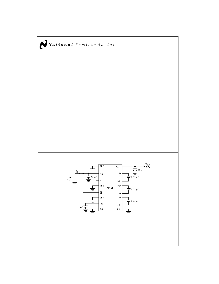
Typical Operating Circuit
DS101037-1
September 1999
LM3352
Regulated
200
mA
Buck-Boost
Switched
Capacitor
DC/DC
Converter
© 1999 National Semiconductor Corporation
DS101037
www.national.com

Connection Diagram
Ordering Information
Order Number
Package Type
NSC Package Drawing
Supplied As
LM3352MTCX-2.5
TSSOP-16
MTC16
2.5k Units, Tape and Reel
LM3352MTC-2.5
TSSOP-16
MTC16
94 Units, Rail
LM3352MTCX-3.0
TSSOP-16
MTC16
2.5k Units, Tape and Reel
LM3352MTC-3.0
TSSOP-16
MTC16
94 Units, Rail
LM3352MTCX-3.3
TSSOP-16
MTC16
2.5k Units, Tape and Reel
LM3352MTC-3.3
TSSOP-16
MTC16
94 Units, Rail
Pin Description
Pin Number
Name
Function
1
GND
Ground
*
2
C3-
Negative Terminal for C3
3
C3+
Positive Terminal for C3
4
C2-
Negative Terminal for C2
5
C2+
Positive Terminal for C2
6
C1-
Negative Terminal for C1
7
C1+
Positive Terminal for C1
8
V
OUT
Regulated Output Voltage
9
GND
Ground
*
10
V
IN
Input Supply Voltage
11
NC
This pin must be left unconnected.
12
GND
Ground
*
13
SD
Active Low CMOS Logic-Level Shutdown Input
14
GND
Ground
*
15
C
FIL
Filter Capacitor; A 1 µF ceramic capacitor is suggested.
16
GND
Ground
*
*
All GND pins of the LM3352 must be connected to the same ground.
DS101037-2
Top View
TSSOP-16 Pin Package
See NS Package Number MTC16
www.national.com
2

Absolute Maximum Ratings
(Note 1)
If Military/Aerospace specified devices are required,
please contact the National Semiconductor Sales Office/
Distributors for availability and specifications.
V
OUT
Pin
-0.5V to 4.5V
All Other Pins
-0.5V to 5.6V
Power Dissipation (T
A
= 25∞C)
(Note 2)
700 mW
T
JMAX
(Note 2)
150∞C
JA
(Note 2)
150∞C/W
Storage Temperature
-65∞C to +150∞C
Lead Temperature (Soldering, 5 sec.)
260∞C
ESD Rating (Note 3)
human body model
machine model
2 kV
100V
Operating Ratings
Input Voltage (V
IN
)
2.5V to 5.5V
Output Voltage (V
OUT
)
1.8V to 4.0V
Ambient Temperature (T
A
) (Note 2)
-40∞C to +85∞C
Junction Temperature (T
J
) (Note 2)
-40∞C to +125∞C
Electrical Characteristics
Limits in standard typeface are for T
J
= 25∞C, and limits in boldface type apply over the full operating temperature range. Unless
otherwise specified: C
1
= C
2
= C
3
= 0.33 µF; C
IN
= 15 µF; C
OUT
= 33 µF; V
IN
= 3.5V.
Parameter
Conditions
Min
Typ
Max
Units
LM3352-2.5
Output Voltage (V
OUT
)
V
IN
= 3.5V; I
LOAD
= 100 mA
2.463
2.5
2.537
V
2.8V
<
V
IN
<
5.5V;
1 mA
<
I
LOAD
<
100 mA
2.425/2.400
2.5
2.575/2.600
3.6V
<
V
IN
<
4.9V;
1 mA
<
I
LOAD
<
200 mA
2.425/2.400
2.5
2.575/2.600
4.9V
<
V
IN
<
5.5V;
1 mA
<
I
LOAD
<
175 mA
2.425/2.400
2.5
2.575/2.600
Efficiency
I
LOAD
= 15 mA
85
%
I
LOAD
= 150 mA, V
IN
= 4.0V
75
Output Voltage Ripple
(Peak-to-Peak)
I
LOAD
= 50 mA
C
OUT
= 33 µF tantalum
75
mV
P-P
LM3352-3.0
Output Voltage (V
OUT
)
V
IN
= 3.5V; I
LOAD
= 100 mA
2.955
3.0
3.045
V
2.5V
<
V
IN
<
5.5V;
1 mA
<
I
LOAD
<
100 mA
2.910/2.880
3.0
3.090/3.120
3.8V
<
V
IN
<
5.5V;
1 mA
<
I
LOAD
<
200 mA
2.910/2.880
3.0
3.090/3.120
Efficiency
I
LOAD
= 15 mA
80
%
I
LOAD
= 150 mA, V
IN
= 4.0V
75
Output Voltage Ripple
(Peak-to-Peak)
I
LOAD
= 50 mA
C
OUT
= 33 µF tantalum
75
mV
P-P
LM3352-3.3
Output Voltage (V
OUT
)
V
IN
= 3.5V; I
LOAD
= 100 mA
3.251
3.3
3.349
V
2.5V
<
V
IN
<
5.5V;
1 mA
<
I
LOAD
<
100 mA
3.201/3.168
3.3
3.399/3.432
4.0V
<
V
IN
<
5.5V;
1 mA
<
I
LOAD
<
200 mA
3.201/3.168
3.3
3.399/3.432
Efficiency
I
LOAD
= 15 mA
90
%
I
LOAD
= 150 mA, V
IN
= 4.0V
80
Output Voltage Ripple
(Peak-to-Peak)
I
LOAD
= 50 mA
C
OUT
= 33 µF tantalum
75
mV
P-P
LM3352-ALL OUTPUT VOLTAGE VERSIONS
Operating Quiescent Current
Measured at Pin V
IN
;
I
LOAD
= 0A (Note 4)
400
500
µA
Shutdown Quiescent Current
SD Pin at 0V (Note 5)
2.5
5
µA
Switching Frequency
0.65
1
1.35
MHz
SD Input Threshold Low
2.5V
<
V
IN
<
5.5V
0.2 V
IN
V
SD Input Threshold High
2.5V
<
V
IN
<
5.5V
0.8 V
IN
V
www.national.com
3

Electrical Characteristics
(Continued)
Limits in standard typeface are for T
J
= 25∞C, and limits in boldface type apply over the full operating temperature range. Un-
less otherwise specified: C
1
= C
2
= C
3
= 0.33 µF; C
IN
= 15 µF; C
OUT
= 33 µF; V
IN
= 3.5V.
Parameter
Conditions
Min
Typ
Max
Units
LM3352-ALL OUTPUT VOLTAGE VERSIONS
SD Input Current
Measured at SD Pin;
SD Pin = V
IN
= 5.5V
0.1
1.0
µA
Note 1: "Absolute Maximum Ratings" indicate limits beyond which damage to the device may occur. Electrical specifications do not apply when operating the device
beyond its rated operating conditions.
Note 2: As long as T
A
+85∞C, all electrical characteristics hold true for the 3.0V and 3.3V options at all current loads and the 2.5V option at all loads when V
IN
5V. For V
IN
>
5V with the 2.5V option, the junction temperature rise above ambient is:
T = 540I
L
-23 where I
L
is in amps. The output current must be derated at
higher ambient temperatures to make sure T
J
does not exceed 150∞C when operating the 2.5V option at V
IN
>
5V.
Note 3: The human body model is a 100 pF capacitor discharged through a 1.5 k
resistor into each pin. The machine model is a 200 pF capacitor discharged di-
rectly into each pin.
Note 4: The V
OUT
pin is forced to 200 mV above the typical V
OUT
. This is to insure that the internal switches are off.
Note 5: The output capacitor C
OUT
is fully discharged before measurement.
Typical Performance Characteristics
Unless otherwise specified T
A
= 25∞C.
V
OUT
vs. V
IN
DS101037-4
V
OUT
vs. V
IN
DS101037-5
V
OUT
vs. V
IN
DS101037-6
V
OUT
vs. V
IN
DS101037-7
www.national.com
4

Typical Performance Characteristics
Unless otherwise specified T
A
= 25∞C. (Continued)
V
OUT
vs. V
IN
DS101037-8
V
OUT
vs. V
IN
DS101037-9
V
OUT
vs. V
IN
DS101037-10
V
OUT
vs. V
IN
DS101037-11
V
OUT
vs. V
IN
DS101037-12
Load Transient Response
DS101037-14
www.national.com
5