
LM3502
Step-Up Converter for White LED Applications
General Description
The LM3502 is a white LED driver for lighting applications.
For dual display or large single white LED string backlighting
applications, the LM3502 provides a complete solution. The
LM3502 contains two internal whitle LED current bypass
FET(Field Effect Transitor) switches that are ideal for con-
troling dual display applications. The while LED current can
be adjusted with a PWM signal directly from a microcontrol-
ler without the need of an RC filter network.
With no external compensation, cycle-by-cycle current limit,
over-voltage protection, and under-voltage protection, the
LM3502 offers superior performance over other application
specific standard product step-up white LED drivers.
Features
n
Drive up to 4, 6, 8 or 10 white LEDs for Dual Display
Backlighting
n
>
80% efficiency
n
Output Voltage Options: 16V , 25V , 35V, and 44V
n
Input Under-Voltage Protection
n
Internal Soft Start Eliminating Inrush Current
n
1 MHz Constant-Switching Frequency
n
Wide Input Voltage: 2.5V to 5.5V
n
Small External Components
n
Low Profile Packages:
<
1 mm Height
-10 Bump MicroSMD
-16 Pin LLP
Applications
n
Dual Display BackLighting in Portable Devices
n
Cellular Phones and PDAs
Typical Application
20131701
FIGURE 1. Blacklight Configuration with 10 White LEDs
September 2005
LM3502
Step-Up
Converter
for
White
LED
Applications
© 2005 National Semiconductor Corporation
DS201317
www.national.com

Connection Diagrams
10-Bump Thin MicroSMD
Package (TLP10)
16-Lead Thin Leadless Leadframe
Package (SQA16A)
20131702
TOP VIEW
20131703
TOP VIEW
Pin Descriptions/Functions
Bump #
Pin #
Name
Description
A1
9
Cntrl
Shutdown Control Connection
B1
7
Fb
Feedback Voltage Connection
C1
6
V
OUT2
Drain Connections of The NMOS and PMOS Field Effect Transistor (FET) Switches
(Figure 2: N2 and P1)
D1
4
V
OUT1
Over-Voltage Protection (OVP) and Source Connection of The PMOS FET Switch
(Figure 2: P1)
D2
2 and 3
Sw
Drain Connection of The Power NMOS Switch (Figure 2: N1)
D3
15 and 16
PGND
Power Ground Connection
C3
14
AGND
Analog Ground Connection
B3
13
V
IN
Supply or Input Voltage Connection
A3
12
En2
NMOS FET Switch Control Connection
A2
10
En1
PMOS FET Switch Control Connection
1
NC
No Connection
5
NC
No Connection
8
NC
No Connection
11
NC
No Connection
DAP
DAP
Die Attach Pad (DAP), must be soldered to the printed circuit board's ground plane for
enhanced thermal dissipation.
Cntrl (Bump A1): Shutdown control pin. When V
Cntrl
is
1.4V, the LM3502 is enabled or ON. When V
Cntrl
is
0.3V,
the LM3502 will enter into shutdown mode operation. The
LM3502 has an internal pull down resistor on the Cntrl pin,
thus the device is normally in the off state or shutdown mode
of operation.
Fb (Bump B1): Output voltage feedback connection. The
white LED string network current is set/programmed using a
resistor from this pin to ground.
V
OUT2
(Bump C1): Drain connections of the internal PMOS
and NMOS FET switches. (Figure 2: P1 and N2). It is rec-
ommended to connect 100nF at V
OUT2
for the LM3502-35V
and LM3502-44 versions if V
OUT2
is not used.
V
OUT1
(Bump D1): Source connection of the internal PMOS
FET switch (Figure 2: P1) and OVP sensing node. The
output capacitor must be connected as close to the device
as possible, between the V
OUT1
pin and ground plane. Also
connect the Schottky diode as close as possible to the
V
OUT1
pin to minimize trace resistance and EMI radiation.
Sw (Bump D2): Drain connection of the internal power
NMOS FET switch. (Figure 2: N1) Minimize the metal trace
length and maximize the metal trace width connected to this
pin to reduce EMI radiation and trace resistance.
PGND (Bump D3): Power ground pin. Connect directly to
the ground plane.
AGND (Bump C3): Analog ground pin. Connect the analog
ground pin directly to the PGND pin.
V
IN
(Bump B3): Supply or input voltage connection pin. The
C
IN
capacitor should be as close to the device as possible,
between the V
IN
pin and ground plane.
En2 (Bump A3): Enable pin for the internal NMOS FET
switch (Figure 2: N2) during device operation. When V
En2
is
LM3502
www.national.com
2

Pin Descriptions/Functions
(Continued)
0.3V, the internal NMOS FET switch turns on and the SUB
display turns off. When V
En2
is
1.4V, the internal NMOS
FET switch turns off and the SUB display turns on. The En2
pin has an internal pull down resistor, thus the internal
NMOS FET switch is normally in the on state of operation
with the SUB display turned off.
If V
En1
and V
En2
are
0.3V and V
Cntrl
is
1.4V, the LM3502
will enter a low I
Q
shutdown mode of operation where all the
internal FET switches are off. If V
OUT2
is not used, En2 must
be grounded or floating and use En1 along with Cntrl, to
enable the device.
En1 (Bump A2): Enable pin for the internal PMOS FET
switch (Figure 2: P1) during device operation. When V
En1
is
0.3V, the internal PMOS FET switch turns on and the MAIN
display is turned off. When V
En1
is
1.4V, the internal PMOS
FET switch turns off and the MAIN display is turned on. The
En1 pin has an internal pull down resistor, thus the internal
PMOS FET switch is normally in the on state of operation
with the MAIN display turned off. If V
En1
and V
En2
are
0.3V
and V
Cntrl
is
1.4V, the LM3502 will enter a low I
Q
shutdown
mode of operation where all the internal FET switches are
off. If V
OUT2
is not used, En2 must be grounded and use En1
a long with Cntrl, to enable the device.
Ordering Information
Voltage Option
Order Number
Package Marking
Supplied As
16
LM3502ITL-16
SANB
250 units, Tape-and-Reel
16
LM3502ITLX-16
SANB
3000 units, Tape-and-Reel
16
LM3502SQ-16
L00048B
250 units, Tape-and-Reel
16
LM3502SQX-16
L00048B
3000 units, Tape-and-Reel
25
LM3502ITL-25
SAPB
250 units, Tape-and-Reel
25
LM3502ITLX-25
SAPB
3000 units, Tape-and-Reel
25
LM3502SQ-25
L00049B
250 units, Tape-and-Reel
25
LM3502SQX-25
L00049B
3000 units, Tape-and-Reel
35
LM3502ITL-35
SARB
250 units, Tape-and-Reel
35
LM3502ITLX-35
SARB
3000 units, Tape-and-Reel
35
LM3502SQ-35
L00044B
250 units, Tape-and-Reel
35
LM3502SQX-35
L00044B
3000 units, Tape-and-Reel
44
LM3502ITL-44
SDLB
250 units, Tape-and-Reel
44
LM3502ITLX-44
SDLB
3000 units, Tape-and-Reel
44
LM3502SQ-44
L00050B
250 units, Tape-and-Reel
44
LM3502SQX-44
L00050B
3000 units, Tape-and-Reel
LM3502
www.national.com
3

Absolute Maximum Ratings
(Notes 6, 1)
If Military/Aerospace specified devices are required,
please contact the National Semiconductor Sales Office/
Distributors for availability and specifications.
V
IN
Pin
-0.3V to +5.5V
Sw Pin
-0.3V to +48V
Fb Pin
-0.3V to +5.5V
Cntrl Pin
-0.3V to +5.5V
V
OUT1
Pin
-0.3V to +48V
V
OUT2
Pin
-0.3V to V
OUT1
En1
-0.3V to +5.5V
En2
-0.3V to +5.5V
Continuous Power Dissipation
Internally Limited
Maximum Junction Temperature
(T
J-MAX)
+150∞C
Storage Temperature Range
-65∞C to +150∞C
ESD Rating (Note 2)
Human Body Model:
Machine Model:
2 kV
200V
Operating Conditions
(Notes 1, 6)
Junction Temperature (T
J
) Range
-40∞C to +125∞C
Ambient Temperature (T
A
) Range
-40∞C to +85∞C
Input Voltage, V
IN
Pin
2.5V to 5.5V
Cntrl, En1, and En2 Pins
0V to 5.5V
Thermal Properties
(Note 4)
Junction-to-Ambient Thermal Resistance (
JA
)
Micro SMD Package
65∞C/W
Leadless Leadframe Package
49∞C/W
Preliminary Electrical Characteristics
(Notes 6, 7)
Limits in standard typeface are for T
J
= 25∞C.
Limits in bold typeface apply over the full operating junction temperature range (-40∞C
T
J
+125∞C). Unless otherwise
specified, V
IN
= 2.5V.
Symbol
Parameter
Conditions
Min
Typ
Max
Units
V
IN
Input Voltage
2.5
5.5
V
I
Q
Non-Switching
Switching
Shutdown
Low I
Q
Shutdown
Fb
>
0.25V
Fb = 0V, Sw Is Floating
Cntrl = 0V
Cntrl = 1.5V, En1 = En2 = 0V
0.5
1.9
0.1
6
1
3
3
15
mA
mA
µA
µA
V
Fb
Feedback Voltage
0.18
0.25
0.3
V
I
CL
NMOS Power Switch
Current Limit
-16, Fb = 0V
-25, Fb = 0V
-35, Fb = 0V
-44, Fb = 0V
250
400
450
450
400
600
750
750
650
800
1050
1050
mA
I
Fb
Feedback Pin Bias
Current (Note 8)
Fb = 0.25V
64
500
nA
F
S
Switching Frequency
0.8
1
1.2
MHz
R
DS(ON)
NMOS Power Switch
ON Resistance
(Figure 2: N1)
I
Sw
= 500 mA
0.55
1.1
R
PDS(ON)
PMOS ON Resistance
of V
OUT1
/V
OUT2
Switch
(Figure 2: N1)
I
PMOS
= 20 mA, En1 = 0V, En2 = 1.5V
5
10
R
NDS(ON)
NMOS ON Resistance
of V
OUT2
/Fb Switch
(Figure 2: N2)
I
NMOS
= 20 mA, En1 = 1.5V, En2 = 0V
2.5
5
D
MAX
Maximum Duty Cycle
Fb = 0V
90
95
%
I
Cntrl
Cntrl Pin Input Bias
Current (Note 3)
Cntrl = 2.5V
Cntrl = 0V
7
0.1
14
µA
I
Sw
Sw Pin Leakage
Current (Note 3)
Sw = 42V, Cntrl = 0V
0.01
5
µA
I
VOUT1
(OFF) V
OUT1
Pin Leakage
Current (Note 3)
V
OUT1
= 14V, Cntrl = 0V (16)
V
OUT1
= 23V, Cntrl = 0V (25)
V
OUT1
= 32V, Cntrl = 0V (35)
V
OUT1
= 42V, Cntrl = 0V (44)
0.1
0.1
0.1
0.1
3
3
3
3
µA
LM3502
www.national.com
4
Preliminary Electrical Characteristics
(Notes 6, 7) Limits in standard typeface are for T
J
= 25∞C.
Limits in bold typeface apply over the full operating junction temperature range (-40∞C
T
J
+125∞C). Unless otherwise
specified, V
IN
= 2.5V. (Continued)
Symbol
Parameter
Conditions
Min
Typ
Max
Units
I
VOUT1
(ON) V
OUT1
Pin Bias
Current (Note 3)
V
OUT1
= 14V, Cntrl = 1.5V (16)
V
OUT1
= 23V, Cntrl = 1.5V (25)
V
OUT1
= 32V, Cntrl = 1.5V (35)
V
OUT1
= 42V, Cntrl = 1.5V (44)
40
50
50
85
80
100
100
140
µA
I
VOUT2
V
OUT2
Pin Leakage
Current (Note 3)
Fb = 0V, Cntrl = 0V, V
OUT2
= 42V
0.1
3
µA
UVP
Under-Voltage
Protection
On Threshold
Off Threshold
2.2
2.4
2.3
2.5
V
OVP
Over-Voltage
Protection (Note 5)
On Threshold (16)
Off Threshold (16)
On Threshold (25)
Off Threshold (25)
On Threshold (35)
Off Threshold (35)
On Threshold (44)
Off Threshold (44)
14.5
14.0
22.5
21.5
32.0
31.0
40.5
39.0
15.5
15
24
23
34
33
42
41
16.5
16.0
25.5
24.5
35.0
34.0
43.5
42.0
V
V
En1
PMOS FET Switch
Enabling Threshold
(Figure 2: P1)
Off Threshold (Display Lighting)
On Threshold (Display Lighting)
1.4
0.8
0.8
0.3
V
V
En2
NMOS FET Switch
Enabling Threshold
(Figure 2: N2)
Off Threshold (Display Lighting)
On Threshold (Display Lighting)
1.4
0.8
0.8
0.3
V
V
Cntrl
Device Enabling
Threshold
Off Threshold
OnThreshold
1.4
0.8
0.8
0.3
V
T
SHDW
Shutdown Delay Time
8
12
16
ms
I
En1
En1 Pin Input Bias
Current
En1 = 2.5V
En1 = 0V
7
0.1
14
µA
I
En2
En2 Pin Input Bias
Current
En2 = 2.5V
En2 = 0V
7
0.1
14
µA
Note 1: Absolute maximum ratings indicate limits beyond which damage to the device may occur. Electrical characteristic specifications do not apply when
operating the device outside of its rated operating conditions.
Note 2: The human body model is a 100 pF capacitor discharged through a 1.5 k
resistor into each pin. The machine model is a 200 pF capacitor discharged
directly into each pin.
Note 3: Current flows into the pin.
Note 4: The maximum allowable power dissipation is a function of the maximum junction temperature, T
J
(MAX), the junction-to-ambient thermal resistance,
JA
,
and the ambient temperature, T
A
. See Thermal Properties for the thermal resistance. The maximum allowable power dissipation at any ambient temperature is
calculated using: P
D
(MAX) = (T
J
(MAX) ≠ T
A
)/
JA
. Exceeding the maximum allowable power dissipation will cause excessive die temperature. For more information
on this topic, please refer to Application Note 1187: Leadless Leadframe Package (LLP) and Application Note 1112 (AN1112) for microSMD chip scale package.
Note 5: The on threshold indicates that the LM3502 is no longer switching or regulating LED current, while the off threshold indicates normal operation.
Note 6: All voltages are with respect to the potential at the GND pin.
Note 7: Min and Max limits are guaranteed by design, test, or statistical analysis. Typical numbers are not guaranteed, but do represent the most likely norm.
Note 8: Current flows out of the pin.
LM3502
www.national.com
5

Block Diagram
20131704
FIGURE 2. Block Diagram
LM3502
www.national.com
6

Detailed Description of Operation
The LM3502 utilizes an asynchronous current mode pulse-
width-modulation (PWM) control scheme to regulate the
feedback voltage over specified load conditions. The DC/DC
converter behaves as a controlled current source for white
LED applications. The operation can best be understood by
referring to the block diagram in Figure 2 for the following
operational explanation. At the start of each cycle, the oscil-
lator sets the driver logic and turns on the internal NMOS
power device, N1, conducting current through the inductor
and reverse biasing the external diode. The white LED cur-
rent is supplied by the output capacitor when the internal
NMOS power device, N1, is turned on. The sum of the error
amplifier's output voltage and an internal voltage ramp are
compared with the sensed power NMOS, N1, switch voltage.
Once these voltages are equal, the PWM comparator will
then reset the driver logic, thus turning off the internal NMOS
power device, N1, and forward biasing the external diode.
The inductor current then flows through the diode to the
white LED load and output capacitor. The inductor current
recharges the output capacitor and supplies the current for
the white LED load. The oscillator then resets the driver logic
again repeating the process. The output voltage of the error
amplifier controls the current through the inductor. This volt-
age will increase for larger loads and decrease for smaller
loads limiting the peak current in the inductor and minimizing
EMI radiation. The duty limit comparator is always opera-
tional, it prevents the internal NMOS power switch, N1, from
being on for more than one oscillator cycle and conducting
large amounts of current. The light load comparator allows
the LM3502 to properly regulate light/small white LED load
currents,
where
regulation
becomes
difficult
for
the
LM3502's primary control loop. Under light load conditions,
the LM3502 will enter into a pulse skipping pulse-frequency-
mode (PFM) of operation where the switching frequency will
vary with the load.
The LM3502 has 2 control pins, En1 and En2, used for
selecting which segment of a single white LED string net-
work is active for dual display applications. En1 controls the
main display (MAIN) segment of the single string white LED
network between pins V
OUT1
and V
OUT2
. En2 controls the
sub display (SUB) segment of the single string white LED
network between the V
OUT2
and Fb. For a quick review of
the LM3502 control pin operational characteristics, see Fig-
ure 3.
When the Cntrl pin is
1.4V, the LM3502 will enter in low I
Q
state if both En1 and En2
0.3V. At this time, both the P1
and N2 FETs will turn off. The output voltage will be a diode
drop below the supply voltage and the soft-start will be reset
limiting the peak inductor current at the next start-up.
The LM3502 is designed to control the LED current with a
PWM signal without the use of an external RC filter. Utilizing
special circuitry, the LM3502 can operate over a large range
of PWM frequencies without restarting the soft-start allowing
for fast recovery at high PWM frequencies. Figure 4
reprsents a PWM signal driving the Cntrl pin where t
L
is
defined as the low time of the signal. The following is true:
∑
If t
L
<
12ms (typical): The device will stop switching
during this time and the soft-start will not be reset allow-
ing LED current PWM control.
∑
If t
L
>
12ms (typical): The device will shutdown and the
soft-start will reset to prevent high peak currents at the
next startup. Both the N2 and P1 switches will turn off.
The LM3502 has dedicated protection circuitry active during
normal operation to protect the integrated circuit (IC) and
external components. The thermal shutdown circuitry turns
off the internal NMOS power device, N1, when the internal
semiconductor junction temperature reaches excessive lev-
els. The LM3502 has a under-voltage protection (UVP) com-
parator that disables the internal NMOS power device when
battery voltages are too low, thus preventing an on state
where the internal NMOS power device conducts large
amounts of current. The over-voltage protection (OVP) com-
parator prevents the output voltage from increasing beyond
the protection limit when the white LED string network is
removed or if there is a white LED failure. OVP allows for the
use of low profile ceramic capacitors at the output. The
current though the internal NMOS power device, N1, is
monitored to prevent peak inductor currents from damaging
the IC. If during a cycle (cycle=1/switching frequency) the
peak inductor current exceeds the current limit for the
LM3502, the internal NMOS power device will be turned off
for the remaining duration of that cycle.
LM3502
www.national.com
7
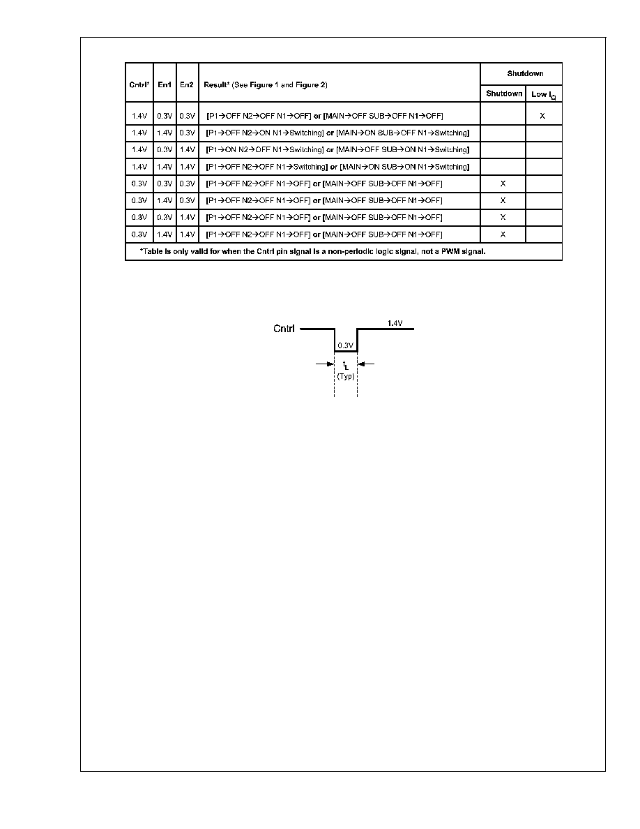
20131705
FIGURE 3. Operational Characteristics Table
20131706
FIGURE 4. Control Signal Waveform
LM3502
www.national.com
8

Typical Performance Characteristics
( Circuit in Figure 1: L = DO1608C-223 and D = MBRM140T3.
Efficiency:
= P
OUT
/P
IN
= [(V
OUT
≠ V
Fb
) * I
OUT
]/[V
IN
* I
IN
]. T
A
= 25∞C, unless otherwise stated.)
I
Q
(Non-Switching) vs V
IN
Switching Frequency vs Temperature
20131707
20131708
I
Q
(Switching) vs V
IN
I
Q
(Switching) vs Temperature
20131709
20131710
10 LED Efficiency vs LED Current
8 LED Efficiency vs LED Current
20131711
20131712
LM3502
www.national.com
9

Typical Performance Characteristics
( Circuit in Figure 1: L = DO1608C-223 and D = MBRM140T3.
Efficiency:
= P
OUT
/P
IN
= [(V
OUT
≠ V
Fb
) * I
OUT
]/[V
IN
* I
IN
]. T
A
= 25∞C, unless otherwise stated.) (Continued)
6 LED Efficiency vs LED Current
4 LED Efficiency vs LED Current
20131713
20131714
Cntrl Pin Current vs Cntrl Pin Voltage
Maximum Duty Cycle vs Temperature
20131715
20131716
En1 Pin Current vs En1 Pin Voltage
En2 Pin Current vs En2 Pin Voltage
20131717
20131718
LM3502
www.national.com
10

Typical Performance Characteristics
( Circuit in Figure 1: L = DO1608C-223 and D = MBRM140T3.
Efficiency:
= P
OUT
/P
IN
= [(V
OUT
≠ V
Fb
) * I
OUT
]/[V
IN
* I
IN
]. T
A
= 25∞C, unless otherwise stated.) (Continued)
V
OUT1
Pin Current vs V
OUT1
Pin Voltage
Power NMOS R
DS(ON)
(Figure 2: N1) vs V
IN
20131719
20131720
NMOS R
DS(ON)
(Figure 2: N2) vs V
IN
PMOS R
DS(ON)
(Figure 2: P1) vs V
IN
20131721
20131722
Feedback Voltage vs Temperature
20131725
LM3502
www.national.com
11

Typical Performance Characteristics
( Circuit in Figure 1: L = DO1608C-223 and D = MBRM140T3.
Efficiency:
= P
OUT
/P
IN
= [(V
OUT
≠ V
Fb
) * I
OUT
]/[V
IN
* I
IN
]. T
A
= 25∞C, unless otherwise stated.) (Continued)
Current Limit (LM3502-16) vs V
IN
Current Limit (LM3502-16) vs Temperature
20131754
20131755
Current Limit (LM3502-25) vs V
IN
Current Limit (LM3502-25) vs Temperature
20131756
20131757
Current Limit (LM3502-35/44) vs Temperature
Current Limit (LM3502-35/44) vs V
IN
20131758
20131729
LM3502
www.national.com
12

Application Information
WHITE LED CURRENT SETTING
The LED current is set using the following equation:
20131730
I
LED
: White LED Current.
V
Fb
: Feedback Pin Voltage. V
Fb
= 0.25V, Typical.
R1:
Currrent Setting Resistor.
WHITE LED DIMMING
For dimming the white LED string with a pulse-width-
modulated (PWM) signal on the Cntrl pin, care must taken to
balance the tradeoffs between audible noise and white LED
brightness control. For best PWM duty cycle vs. white LED
current linearity, the PWM frequency should be between
200Hz and 500Hz. Other PWM frequencies can be used, but
the linearity over input voltage and duty cycle variation will
not be as good as what the 200Hz to 500Hz PWM frequency
spectrum provides. To minimize audible noise interference, it
is recommended that a output capacitor with minimal sus-
ceptibility to piezoelectric induced stresses be used for the
particular applications that require minimal or no audible
noise interference.
If V
OUT2
is not used , En2 must be grounded
20131735
FIGURE 5.
LM3502
www.national.com
13

Application Information
(Continued)
CONTINUOUS AND DISCONTINUOUS MODES OF
OPERATION
Since the LM3502 is a constant frequency pulse-width-
modulated step-up regulator, care must be taken to make
sure the maximum duty cycle specification is not violated.
The duty cycle equation depends on which mode of opera-
tion the LM3502 is in. The two operational modes of the
LM3502 are continuous conduction mode (CCM) and dis-
continuous conduction mode (DCM). Continuous conduction
mode refers to the mode of operation where during the
switching cycle, the inductor current never goes to and stays
at zero for any significant amount of time during the switch-
ing cycle. Discontinuous conduction mode refers to the
mode of operation where during the switching cycle, the
inductor current goes to and stays at zero for a significant
amount of time during the switching cycle. Figure 6 illus-
trates the threshold between CCM and DCM operation. In
Figure 6, the inductor current is right on the CCM/DCM
operational threshold. Using this as a reference, a factor can
be introduced to calculate when a particular application is in
CCM or DCM operation. R is a CCM/DCM factor we can use
to compute which mode of operation a particular application
is in. If R is
1, then the application is operating in CCM.
Conversely, if R is
<
1, the application is operating in DCM.
The R factor inequalities are a result of the components that
make up the R factor. From Figure 6, the R factor is equal to
the average inductor current, I
L
(avg), divided by half the
inductor ripple current,
i
L
. Using Figure 6 the following
equation can be used to compute R factor:
20131737
20131738
20131739
20131740
V
IN
:
Input Voltage.
V
OUT
:
Output Voltage.
Eff:
Efficiency of the LM3502.
Fs:
Switching Frequency.
I
OUT
:
White LED Current/Load Current.
L:
Inductance Magnitude/Inductor Value.
D:
Duty Cycle for CCM Operation.
i
L
:
Inductor Ripple Current
I
L
(avg): Average Inductor Current
For CCM operation, the duty cycle can be computed with:
20131741
20131742
D:
Duty Cycle for CCM Operation.
V
OUT
: Output Voltage.
V
IN
:
Input Voltage.
For DCM operation, the duty cycle can be computed with:
20131743
20131736
FIGURE 6. Inductor Current Waveform
LM3502
www.national.com
14

Application Information
(Continued)
20131744
D:
Duty Cycle for DCM Operation.
V
OUT
: Output Voltage.
V
IN
:
Input Voltage.
I
OUT
:
White LED Current/Load Current.
Fs:
Switching Frequency.
L:
Inductor Value/Inductance Magnitude.
INDUCTOR SELECTION
In order to maintain inductance, an inductor used with the
LM3502 should have a saturation current rating larger than
the peak inductor current of the particular application. Induc-
tors with low DCR values contribute decreased power losses
and increased efficiency. The peak inductor current can be
computed for both modes of operation: CCM and DCM.
The cycle-by-cycle peak inductor current for CCM operation
can be computed with:
20131745
20131746
V
IN
:
Input Voltage.
Eff:
Efficiency of the LM3502.
Fs:
Switching Frequency.
I
OUT
:
White LED Current/Load Current.
L:
Inductance Magnitude/Inductor Value.
D:
Duty Cycle for CCM Operation.
I
PEAK
:
Peak Inductor Current.
i
L
:
Inductor Ripple Current.
I
L
(avg): Average Inductor Current.
The cycle-by-cycle peak inductor current for DCM operation
can be computed with:
20131747
V
IN
:
Input Voltage.
Fs:
Switching Frequency.
L:
Inductance Magnitude/Inductor Value.
D:
Duty Cycle for DCM Operation.
I
PEAK
: Peak Inductor Current.
The minimum inductance magnitude/inductor value for the
LM3502 can be calculated using the following, which is only
valid when the duty cycle is
>
0.5:
20131748
D:
Duty Cycle.
D:
1≠D.
R
DS(ON)
: NMOS Power Switch ON Resistance.
V
IN
:
Input Voltage.
L:
Inductance Magnitude/Inductor Value.
This equation gives the value required to prevent subhar-
monic oscillations. The result of this equation and the induc-
tor average and ripple current should be accounted for when
choosing an inductor value.
Some recommended inductor manufacturers included but
are not limited to:
CoilCraft
DO1608C-223
www.coilcraft.com
DT1608C-223
CAPACITOR SELECTION
Multilayer ceramic capacitors are the best choice for use
with the LM3502. Multilayer ceramic capacitors have the
lowest equivalent series resistance (ESR). Applied voltage
or DC bias, temperature, dielectric material type (X7R, X5R,
Y5V, etc), and manufacturer component tolerance have an
affect on the true or effective capacitance of a ceramic
capacitor. Be aware of how your application will affect a
particular ceramic capacitor by analyzing the aforemen-
tioned factors of your application. Before selecting a capaci-
tor always consult the capacitor manufacturer's data curves
to verify the effective or true capacitance in your application.
INPUT CAPACITOR SELECTION
The input capacitor serves as an energy reservoir for the
inductor. In addition to acting as an energy reservoir for the
inductor the input capacitor is necessary for the reduction in
input voltage ripple and noise experienced by the LM3502.
The reduction in input voltage ripple and noise helps ensure
the LM3502's proper operation, and reduces the effect of the
LM3502 on other devices sharing the same supply voltage.
To ensure low input voltage ripple, the input capacitor must
have an extremely low ESR. As a result of the low input
voltage ripple requirement multilayer ceramic capacitors are
the best choice. A minimum capacitance of 2.0 µF is required
for normal operation, so consult the capacitor manufactur-
er's data curves to verify whether the minimum capacitance
requirement is going to be achieved for a particular applica-
tion.
OUTPUT CAPACITOR SELECTION
The output capacitor serves as an energy reservoir for the
white LED load when the internal power FET switch (Figure
2: N1) is on or conducting current. The requirements for the
output capacitor must include worst case operation such as
when the load opens up and the LM3502 operates in over-
voltage protection (OVP) mode operation. A minimum ca-
pacitance of 0.5µF is required to ensure normal operation.
Consult the capacitor manufacturer's data curves to verify
whether the minimum capacitance requirement is going to
be achieved for a particular application.
Some recommended capacitor manufacturers included but
are not limited to:
LM3502
www.national.com
15

Application Information
(Continued)
Taiyo
Yuden
GMK212BJ105MD
(0805/35V)
www.t-yuden.com
muRata
GRM40-035X7R105K
(0805/50V)
www.murata.com
TDK
C3216X7R1H105KT
(1206/50V)
www.tdktca.com
C3216X7R1C475K
(1206/16V)
AVX
08053D105MAT
(0805/25V)
www.avxcorp.com
08056D475KAT
(0805/6.3V)
1206ZD475MAT
(1206/10V)
DIODE SELECTION
To maintain high efficiency it is recommended that the aver-
age current rating (I
F
or I
O
) of the selected diode should be
larger than the peak inductor current (I
Lpeak
). At the mini-
mum, the average current rating of the diode should be
larger than the maximum LED current. To maintain diode
integrity the peak repetitive forward current (I
FRM
) must be
greater than or equal to the peak inductor current (I
Lpeak
).
Diodes with low forward voltage ratings (V
F
) and low junction
capacitance magnitudes (C
J
or C
T
or C
D
) are conducive to
high efficiency. The chosen diode must have a reverse
breakdown voltage rating (V
R
and/or V
RRM
) that is larger
than the output voltage (V
out
). No matter what type of diode
is chosen, Schottky or not, certain selection criteria must be
followed:
1.
V
R
and V
RRM
>
V
OUT
2.
I
F
or I
O
I
LOAD
or I
OUT
3.
I
FRM
I
Lpeak
Some recommended diode manufacturers included but are
not limited to:
Vishay
SS12(1A/20V)
www.vishay.com
SS14(1A/40V)
SS16(1A/60V)
On
Semiconductor
MBRM120E
(1A/20V)
www.onsemi.com
MBRS1540T3
(1.5A/40V)
MBR240LT
(2A/40V)
Central
Semiconductor
CMSH1- 40M
(1A/40V)
www.centralsemi.com
SHUTDOWN AND START-UP
On startup, the LM3502 contains special circuitry that limits
the peak inductor current which prevents large current
spikes from loading the battery or power supply. When Cntrl
1.4V and both the En1 and En2 signals are less than 0.3V,
the LM3502 will enter a low I
Q
state and regulation will end.
During this low I
Q
mode the output voltage is a diode drop
below the supply voltage and the soft-start will be reset to
limit the peak inductor current at the next startup. When both
En1 and En2 are less than 0.3V, the P1 PMOS and N2
NMOS switches will turn off.
When Cntrl
<
0.3V for more than 12ms, typicaly, the LM3502
will shutdown and the output voltage will be a diode drop
below the supply voltage. If the Cntrl pin is low for more than
12ms, the soft-start will reset to limit the peak inductor cur-
rent at the next startup.
When Cntrl is
<
0.3 but for less than 12ms, typically, the
device will not shutdown and reset the soft-start but shut off
the NMOS N1 Power Device to allow for PWM contrl of the
LED current.
THERMAL SHUTDOWN
The LM3502 stops regulating when the internal semiconduc-
tor junction temperature reaches approximately 140∞C. The
internal thermal shutdown has approximately 20∞C of hyster-
esis which results in the LM3502 turning back on when the
internal semiconductor junction temperature reaches 120∞C.
When the thermal shutdown temperature is reached, the
softstart is reset to prevent inrush current when the die
temperature cools.
UNDER VOLTAGE PROTECTION
The LM3503 contains protection circuitry to prevent opera-
tion for low input supply voltages. When Vin drops below
2.3V, typically the LM3502 will no longer regulate. In this
mode, the output volage will be one diode drop below Vin
and the softstart will be reset. When Vin increases above
2.4V, typically, the device will begin regulating again.
OVER VOLTAGE PROTECTION
The LM3502 contains dedicated circuitry for monitoring the
output voltage. In the event that the LED network is discon-
nected from the LM3502, the output voltage will increase
and be limited to 15.5V(typ.) for the 16V version , 24V(typ.)
for the 25V version, 34V(typ.) for the 35V version and
42V(typ.) for the 44V version (see eletrical table for more
details). In the event that the network is reconnected, regu-
lation will resume at the appropriate output voltage.
LAYOUT CONSIDERATIONS
All components, except for the white LEDs, must be placed
as close as possible to the LM3502. The die attach pad
(DAP) must be soldered to the ground plane.
The input bypass capacitor C
IN
, as shown in Figure 1, must
be placed close to the IC and connect between the V
IN
and
PGND pins. This will reduce copper trace resistance which
effects input voltage ripple of the IC. For additional input
voltage filtering, a 100nF bypass capacitor can be placed in
parallel with C
IN
to shunt any high frequency noise to
ground. The output capacitor, C
OUT
, must be placed close to
the IC and be connected between the V
OUT1
and PGND
pins. Any copper trace connections for the C
OUT
capacitor
can increase the series resistance, which directly effects
output voltage ripple and efficiency. The current setting re-
sistor, R1, should be kept close to the Fb pin to minimize
copper trace connections that can inject noise into the sys-
tem. The ground connection for the current setting resistor
network should connect directly to the PGND pin. The AGND
pin should be tied directly to the PGND pin. Trace connec-
tions made to the inductor should be minimized to reduce
power dissipation and increase overall efficiency while re-
ducing EMI radiation. For more details regarding layout
guidelines for switching regulators, refer to Applications Note
AN-1149.
LM3502
www.national.com
16

Physical Dimensions
inches (millimeters) unless otherwise noted
16-Lead Thin Leadless Leadframe Package
NS Package Number SQA16A
TLP10: 10-Bump Thin Micro SMD
X1 = 1.958 mm
X2 = 2.135 mm
X3 = 0.6 mm
NS Package No. TLP10
LM3502
www.national.com
17

Notes
National does not assume any responsibility for use of any circuitry described, no circuit patent licenses are implied and National reserves
the right at any time without notice to change said circuitry and specifications.
For the most current product information visit us at www.national.com.
LIFE SUPPORT POLICY
NATIONAL'S PRODUCTS ARE NOT AUTHORIZED FOR USE AS CRITICAL COMPONENTS IN LIFE SUPPORT DEVICES OR SYSTEMS
WITHOUT THE EXPRESS WRITTEN APPROVAL OF THE PRESIDENT AND GENERAL COUNSEL OF NATIONAL SEMICONDUCTOR
CORPORATION. As used herein:
1. Life support devices or systems are devices or systems
which, (a) are intended for surgical implant into the body, or
(b) support or sustain life, and whose failure to perform when
properly used in accordance with instructions for use
provided in the labeling, can be reasonably expected to result
in a significant injury to the user.
2. A critical component is any component of a life support
device or system whose failure to perform can be reasonably
expected to cause the failure of the life support device or
system, or to affect its safety or effectiveness.
BANNED SUBSTANCE COMPLIANCE
National Semiconductor manufactures products and uses packing materials that meet the provisions of the Customer Products
Stewardship Specification (CSP-9-111C2) and the Banned Substances and Materials of Interest Specification (CSP-9-111S2) and contain
no ``Banned Substances'' as defined in CSP-9-111S2.
Leadfree products are RoHS compliant.
National Semiconductor
Americas Customer
Support Center
Email: new.feedback@nsc.com
Tel: 1-800-272-9959
National Semiconductor
Europe Customer Support Center
Fax: +49 (0) 180-530 85 86
Email: europe.support@nsc.com
Deutsch Tel: +49 (0) 69 9508 6208
English
Tel: +44 (0) 870 24 0 2171
FranÁais Tel: +33 (0) 1 41 91 8790
National Semiconductor
Asia Pacific Customer
Support Center
Email: ap.support@nsc.com
National Semiconductor
Japan Customer Support Center
Fax: 81-3-5639-7507
Email: jpn.feedback@nsc.com
Tel: 81-3-5639-7560
www.national.com
LM3502
Step-Up
Converter
for
White
LED
Applications