 | –≠–ª–µ–∫—Ç—Ä–æ–Ω–Ω—ã–π –∫–æ–º–ø–æ–Ω–µ–Ω—Ç: LM4250CN | –°–∫–∞—á–∞—Ç—å:  PDF PDF  ZIP ZIP |
LM4250
Programmable Operational Amplifier
General Description
The LM4250 and LM4250C are extremely versatile program-
mable monolithic operational amplifiers. A single external
master bias current setting resistor programs the input bias
current, input offset current, quiescent power consumption,
slew rate, input noise, and the gain-bandwidth product. The
device is a truly general purpose operational amplifier.
The LM4250C is identical to the LM4250 except that the
LM4250C has its performance guaranteed over a 0∞C to
+70∞C temperature range instead of the -55∞C to +125∞C
temperature range of the LM4250.
Features
n
±
1V to
±
18V power supply operation
n
3 nA input offset current
n
Standby power consumption as low as 500 nW
n
No frequency compensation required
n
Programmable electrical characteristics
n
Offset voltage nulling capability
n
Can be powered by two flashlight batteries
n
Short circuit protection
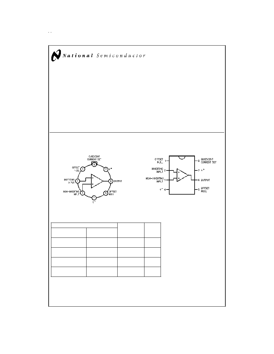
Connection Diagrams
Ordering Information
Temperature Range
Package
NSC
Military
Commercial
Package
-55∞C
T
A
+125∞C
0∞C
T
A
+70∞C
Number
LM4250CN
8-Pin
N08E
Molded DIP
LM4250CM
8-Pin
M08A
Surface Mount
LM4250J
8-Pin
J08E
LM4250J-MIL
Ceramic DIP
LM4250H
LM4250CH
8-Pin
H08C
LM4250H-MIL
Metal Can
Metal Can Package
DS009300-2
Top View
Dual-In-Line Package
DS009300-5
Top View
May 1998
LM4250
Programmable
Operational
Amplifier
© 1999 National Semiconductor Corporation
DS009300
www.national.com

Absolute Maximum Ratings
(Note 1)
If Military/Aerospace specified devices are required,
please contact the National Semiconductor Sales Office/
Distributors for availability and specifications.
(Note 3)
LM4250
LM4250C
Supply Voltage
±
18V
±
18V
Operating Temp. Range
-55∞C
T
A
+125∞C
0∞C
T
A
+70∞C
Differential Input Voltage
±
30V
±
30V
Input Voltage (Note 2)
±
15V
±
15V
I
SET
Current
150 nA
150 nA
Output Short Circuit Duration
Continuous
Continuous
T
JMAX
H-Package
150∞C
100∞C
N-Package
100∞C
J-Package
150∞C
100∞C
M-Package
100∞C
Power Dissipation at T
A
= 25∞C
H-Package (Still Air)
500 mW
300 mW
(400 LF/Min Air Flow)
1200 mW
1200 mW
N-Package
500 mW
J-Package
1000 mW
600 mW
M-Package
350 mW
Thermal Resistance (Typical)
JA
H-Package (Still Air)
165∞C/W
165∞C/W
(400 LF/Min Air Flow)
65∞C/W
65∞C/W
N-Package
130∞C/W
J-Package
108∞C/W
108∞C/W
M-Package
190∞C/W
(Typical)
JC
H-Package
21∞C/W
21∞C/W
Storage Temperature Range
-65∞C to +150∞C
-65∞C to +150∞C
Soldering Information
Dual-In-Line Package
Soldering (10 seconds)
260∞C
Small Outline Package
Vapor Phase (60 seconds)
215∞C
Infrared (15 seconds)
220∞C
See AN-450 "Surface Mounting Methods and Their Effect
on Product Reliability" for other methods of soldering
surface mount devices.
ESD tolerance (Note 4)
800V
Note 1: "Absolute Maximum Ratings" indicate limits beyond which damage
to the device may occur. Operating Ratings indicate conditions for which the
device is functional, but do not guarantee specific performance limits.
Note 2: For supply voltages less than
±
15V, the absolute maximum input
voltage is equal to the supply voltage.
Note 3: Refer to RETS4250X for military specifications.
Note 4: Human body model, 1.5 k
in series with 100 pF.
www.national.com
2
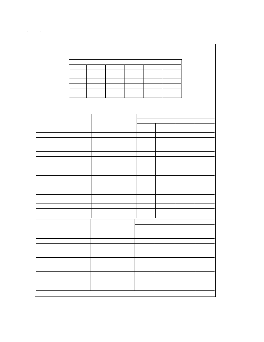
Resistor Biasing
Set Current Setting Resistor to V
-
I
SET
V
S
0.1 µA
0.5 µA
1.0 µA
5 µA
10 µA
±
1.5V
25.6 M
5.04 M
2.5 M
492 k
244 k
±
3.0V
55.6 M
11.0 M
5.5 M
1.09 M
544 k
±
6.0V
116 M
23.0 M
11.5 M
2.29 M
1.14 M
±
9.0V
176 M
35.0 M
17.5 M
3.49 M
1.74 M
±
12.0V
236 M
47.0 M
23.5 M
4.69 M
2.34 M
±
15.0V
296 M
59.0 M
29.5 M
5.89 M
2.94 M
Electrical Characteristics
LM4250 (-55∞C
T
A
+125∞C unless otherwise specified.) T
A
= T
J
V
S
=
±
1.5V
Parameter
Conditions
I
SET
= 1 µA
I
SET
= 10 µA
Min
Max
Min
Max
V
OS
R
S
100 k
, T
A
= 25∞C
3 mV
5 mV
I
OS
T
A
= 25∞C
3 nA
10 nA
I
bias
T
A
= 25∞C
7.5 nA
50 nA
Large Signal Voltage
R
L
= 100 k
, T
A
= 25∞C
40k
Gain
V
O
=
±
0.6V, R
L
= 10 k
50k
Supply Current
T
A
= 25∞C
7.5 µA
80 µA
Power Consumption
T
A
= 25∞C
23 µW
240 µW
V
OS
R
S
100 k
4 mV
6 mV
I
OS
T
A
= +125∞C
5 nA
10 nA
T
A
= -55∞C
3 nA
10 nA
I
bias
7.5 nA
50 nA
Input Voltage Range
±
0.6V
±
0.6V
Large Signal Voltage Gain
V
O
=
±
0.5V, R
L
= 100 k
30k
R
L
= 10 k
30k
Output Voltage Swing
R
L
= 100 k
±
0.6V
R
L
= 10 k
±
0.6V
Common Mode Rejection Ratio
R
S
10 k
70 dB
70 dB
Supply Voltage Rejection Ratio
R
S
10 k
76 dB
76 dB
Supply Current
8 µA
90 µA
V
S
=
±
15V
Parameter
Conditions
I
SET
= 1 µA
I
SET
= 10 µA
Min
Max
Min
Max
V
OS
R
S
100 k
, T
A
= 25∞C
3 mV
5 mV
I
OS
T
A
= 25∞C
3 nA
10 nA
I
bias
T
A
= 25∞C
7.5 nA
50 nA
Large Signal Voltage
R
L
= 100 k
, T
A
= 25∞C
100k
Gain
V
O
=
±
10V, R
L
= 10 k
100k
Supply Current
T
A
= 25∞C
10 µA
90 µA
Power Consumption
T
A
= 25∞C
300 µW
2.7 mW
V
OS
R
S
100 k
4 mV
6 mV
I
OS
T
A
= +125∞C
25 nA
25 nA
T
A
= -55∞C
3 nA
10 nA
I
bias
7.5 nA
50 nA
Input Voltage Range
±
13.5V
±
13.5V
www.national.com
3
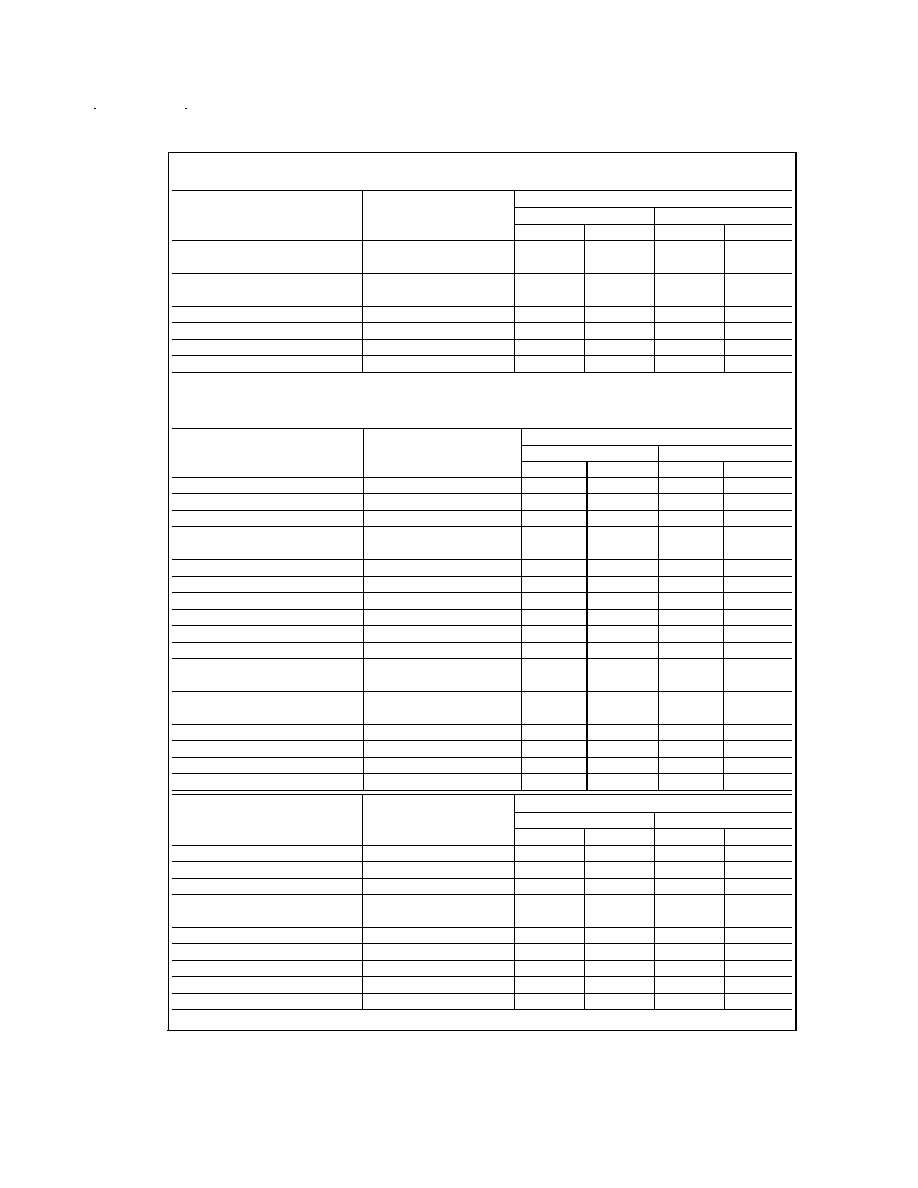
Electrical Characteristics
(Continued)
V
S
=
±
15V
Parameter
Conditions
I
SET
= 1 µA
I
SET
= 10 µA
Min
Max
Min
Max
Large Signal Voltage
V
O
=
±
10V, R
L
= 100 k
50k
Gain
R
L
= 10 k
50k
Output Voltage Swing
R
L
= 100 k
±
12V
R
L
= 10 k
±
12V
Common Mode Rejection Ratio
R
S
10 k
70 dB
70 dB
Supply Voltage Rejection Ratio
R
S
10 k
76 dB
76 dB
Supply Current
11 µA
100 µA
Power Consumption
330 µW
3 mW
Electrical Characteristics
LM4250C (0∞C
T
A
+70∞C unless otherwise specified.) T
A
= T
J
V
S
=
±
1.5V
Parameter
Conditions
I
SET
= 1 µA
I
SET
= 10 µA
Min
Max
Min
Max
V
OS
R
S
100 k
, T
A
= 25∞C
5 mV
6 mV
I
OS
T
A
= 25∞C
6 nA
20 nA
I
bias
T
A
= 25∞C
10 nA
75 nA
Large Signal Voltage Gain
R
L
= 100 k
, T
A
= 25∞C
25k
V
O
=
±
0.6V, R
L
= 10 k
25k
Supply Current
T
A
= 25∞C
8 µA
90 µA
Power Consumption
T
A
= 25∞C
24 µW
270 µW
V
OS
R
S
10 k
6.5 mV
7.5 mV
I
OS
8 nA
25 nA
I
bias
10 nA
80 nA
Input Voltage Range
±
0.6V
±
0.6V
Large Signal Voltage
V
O
=
±
0.5V, R
L
= 100 k
25k
Gain
R
L
= 10 k
25k
Output Voltage Swing
R
L
= 100 k
±
0.6V
R
L
= 10 k
±
0.6V
Common Mode Rejection Ratio
R
S
10 k
70 dB
70 dB
Supply Voltage Rejection Ratio
R
S
10 k
74 dB
74 dB
Supply Current
8 µA
90 µA
Power Consumption
24 µW
270 µW
V
S
=
±
15V
Parameter
Conditions
I
SET
= 1 µA
I
SET
= 10 µA
Min
Max
Min
Max
V
OS
R
S
100 k
, T
A
= 25∞C
5 mV
6 mV
I
OS
T
A
= 25∞C
6 nA
20 nA
I
bias
T
A
= 25∞C
10 nA
75 nA
Large Signal Voltage
R
L
= 100 k
, T
A
= 25∞C
60k
Gain
V
O
=
±
10V, R
L
= 10 k
60k
Supply Current
T
A
= 25∞C
11 µA
100 µA
Power Consumption
T
A
= 25∞C
330 µW
3 mW
V
OS
R
S
100 k
6.5 mV
7.5 mV
I
OS
8 nA
25 nA
I
bias
10 nA
80 nA
www.national.com
4
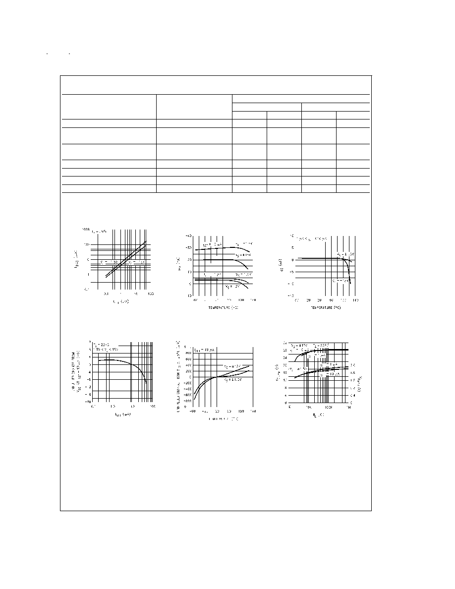
Electrical Characteristics
(Continued)
V
S
=
±
15V
Parameter
Conditions
I
SET
= 1 µA
I
SET
= 10 µA
Min
Max
Min
Max
Input Voltage Range
±
13.5V
±
13.5V
Large Signal Voltage
V
O
=
±
10V, R
L
= 100 k
50k
Gain
R
L
= 10 k
50k
Output Voltage Swing
R
L
= 100 k
±
12V
R
L
= 10 k
±
12V
Common Mode Rejection Ratio
R
S
10 k
70 dB
70 dB
Supply Voltage Rejection Ratio
R
S
10 k
74 dB
74 dB
Supply Current
11 µA
100 µA
Power Consumption
330 µW
3 mW
Typical Performance Characteristics
Input Bias Current vs I
SET
DS009300-15
Input Bias Current vs
Temperature
DS009300-16
Input Offset Current vs
Temperature
DS009300-17
Unnulled Input Offset Voltage
Change vs I
SET
DS009300-18
Unnulled Input Offset Voltage
Change vs Temperature
DS009300-19
Peak to Peak Output Voltage
Swing vs Load Resistance
DS009300-20
www.national.com
5

Typical Performance Characteristics
(Continued)
Peak to Peak Output Voltage
Swing vs Supply Voltage
DS009300-21
Quiescent Current (I
q
) vs
Temperature
DS009300-22
Quiescent Current (I
q
) vs I
SET
DS009300-23
Slew Rate vs I
SET
DS009300-24
Gain Bandwidth Product
vs I
SET
DS009300-25
Open Loop Voltage Gain
vs I
SET
DS009300-26
Phase Margin vs I
SET
DS009300-27
Input Noise Current (I
n
) and
Voltage (E
n
) vs Frequency
DS009300-28
R
SET
vs I
SET
DS009300-29
www.national.com
6
Typical Applications
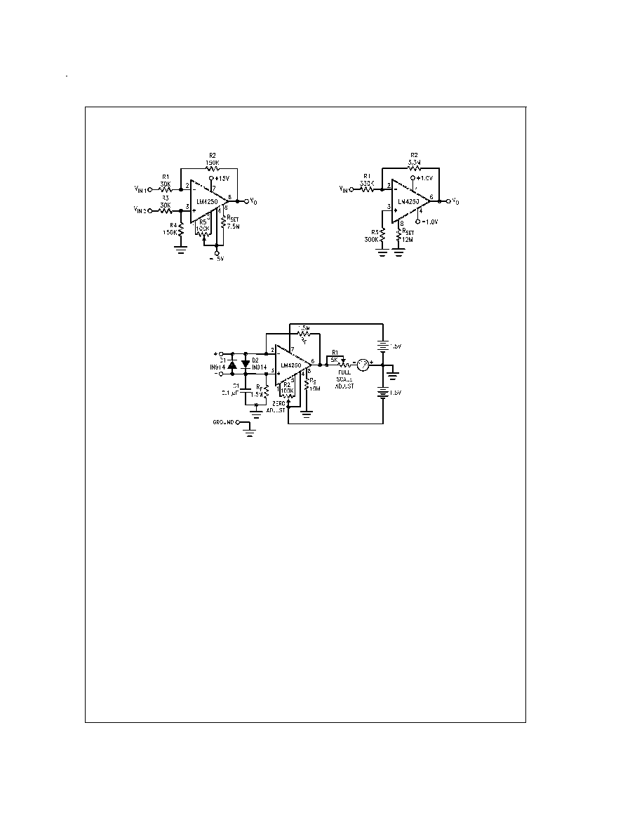
X5 Difference Amplifier
DS009300-3
Quiescent P
D
= 0.6 mW
500 Nano-Watt X10 Amplifier
DS009300-4
Quiescent P
D
= 500 nW
Floating Input Meter Amplifier
100 nA full Scale
DS009300-8
Quiescent P
D
= 1.8 µW
*Meter movement (0≠100 µA, 2 k
) marked for 0≠100 nA full scale.
www.national.com
7
Typical Applications
(Continued)
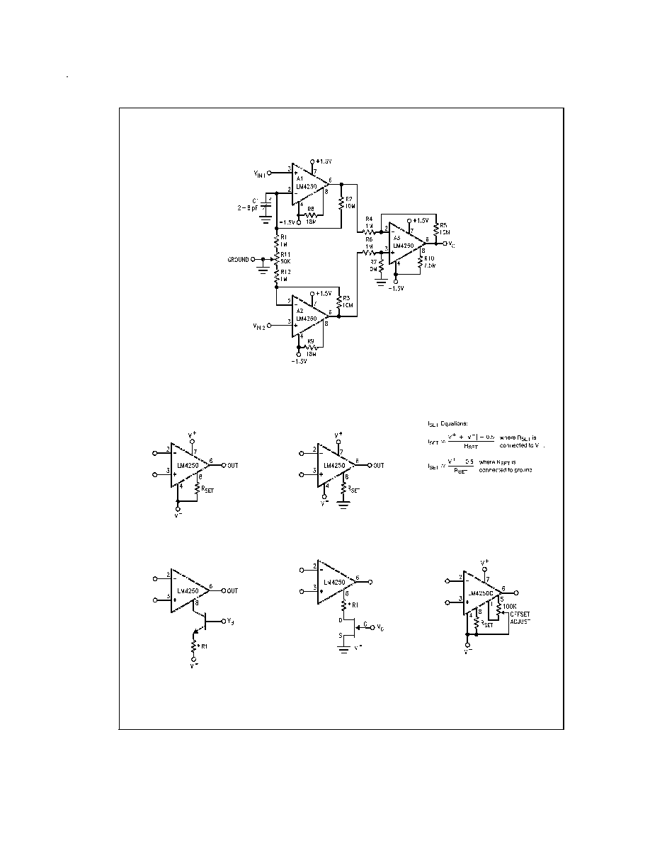
X100 Instrumentation Amplifier 10 µW
DS009300-9
Note 5: Quiescent P
D
= 10 µW.
Note 6: R2, R3, R4, R5, R6 and R7 are 1% resistors.
Note 7: R11 and C1 are for DC and AC common mode rejection adjustments.
R
SET
Connected to V
-
DS009300-10
R
SET
Connected to Ground
DS009300-11
DS009300-30
Transistor Current Sourcing
Biasing
DS009300-12
*R1 limits I
SET
maximum
FET Current Sourcing Biasing
DS009300-13
Offset Null Circuit
DS009300-14
www.national.com
8

Schematic Diagram
DS009300-1
www.national.com
9
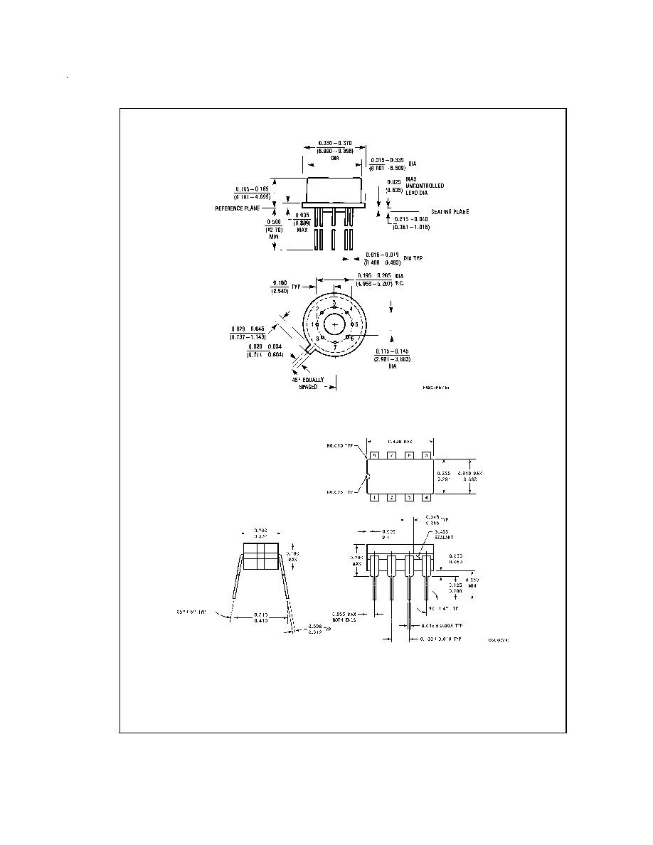
Physical Dimensions
inches (millimeters) unless otherwise noted
Metal Can Package (H)
Order Number LM4250H, LM4250CH or LM4250H-MIL
NS Package Number H08C
Ceramic Dual-In-Line Package (J)
Order Number LM4250J, or LM4250J-MIL
NS Package Number J08A
www.national.com
10

Physical Dimensions
inches (millimeters) unless otherwise noted (Continued)
Small Outline Package (M)
Order Number LM4250M
NS Package Number M08A
Molded Dual-In-Line Package (N)
Order Number LM4250CN
NS Package Number N08E
www.national.com
11

Notes
LIFE SUPPORT POLICY
NATIONAL'S PRODUCTS ARE NOT AUTHORIZED FOR USE AS CRITICAL COMPONENTS IN LIFE SUPPORT
DEVICES OR SYSTEMS WITHOUT THE EXPRESS WRITTEN APPROVAL OF THE PRESIDENT OF NATIONAL
SEMICONDUCTOR CORPORATION. As used herein:
1. Life support devices or systems are devices or
systems which, (a) are intended for surgical implant
into the body, or (b) support or sustain life, and
whose failure to perform when properly used in
accordance with instructions for use provided in the
labeling, can be reasonably expected to result in a
significant injury to the user.
2. A critical component is any component of a life
support device or system whose failure to perform
can be reasonably expected to cause the failure of
the life support device or system, or to affect its
safety or effectiveness.
National Semiconductor
Corporation
Americas
Tel: 1-800-272-9959
Fax: 1-800-737-7018
Email: support@nsc.com
National Semiconductor
Europe
Fax: +49 (0) 1 80-530 85 86
Email: europe.support@nsc.com
Deutsch Tel: +49 (0) 1 80-530 85 85
English
Tel: +49 (0) 1 80-532 78 32
FranÁais Tel: +49 (0) 1 80-532 93 58
Italiano
Tel: +49 (0) 1 80-534 16 80
National Semiconductor
Asia Pacific Customer
Response Group
Tel: 65-2544466
Fax: 65-2504466
Email: sea.support@nsc.com
National Semiconductor
Japan Ltd.
Tel: 81-3-5639-7560
Fax: 81-3-5639-7507
www.national.com
LM4250
Programmable
Operational
Amplifier
National does not assume any responsibility for use of any circuitry described, no circuit patent licenses are implied and National reserves the right at any time without notice to change said circuitry and specifications.