LM4908 Boomer ® Audio Power Amplifier Series 10kV ESD Rated, Dual 120 mW Headphone Amplifier
LM4908
10kV ESD Rated, Dual 120 mW Headphone Amplifier
General Description
The LM4908 is a dual audio power amplifier capable of
delivering 120mW per channel of continuous average power
into a 16
load with 0.1% (THD+N) from a 5V power supply.
Boomer audio power amplifiers were designed specifically to
provide high quality output power with a minimal amount of
external components using surface mount packaging. Since
the LM4908 does not require bootstrap capacitors or snub-
ber networks, it is optimally suited for low-power portable
systems.
The unity-gain stable LM4908 can be configured by external
gain-setting resistors.
Key Specifications
j
THD+N at 1kHz at 120mW
continuous average output power
into 16
0.1% (typ)
j
THD+N at 1kHz at 75mW
continuous average output power
into 32
0.1% (typ)
j
Output power at 0.1% THD+N
at 1kHz into 32
75mW (typ)
Features
n
Up to 10kV ESD protection on all pins
n
MSOP, SOP, and LLP surface mount packaging
n
Switch on/off click suppression
n
Excellent power supply ripple rejection
n
Unity-gain stable
n
Minimum external components
Applications
n
Headphone Amplifier
n
Personal Computers
n
Portable electronic devices
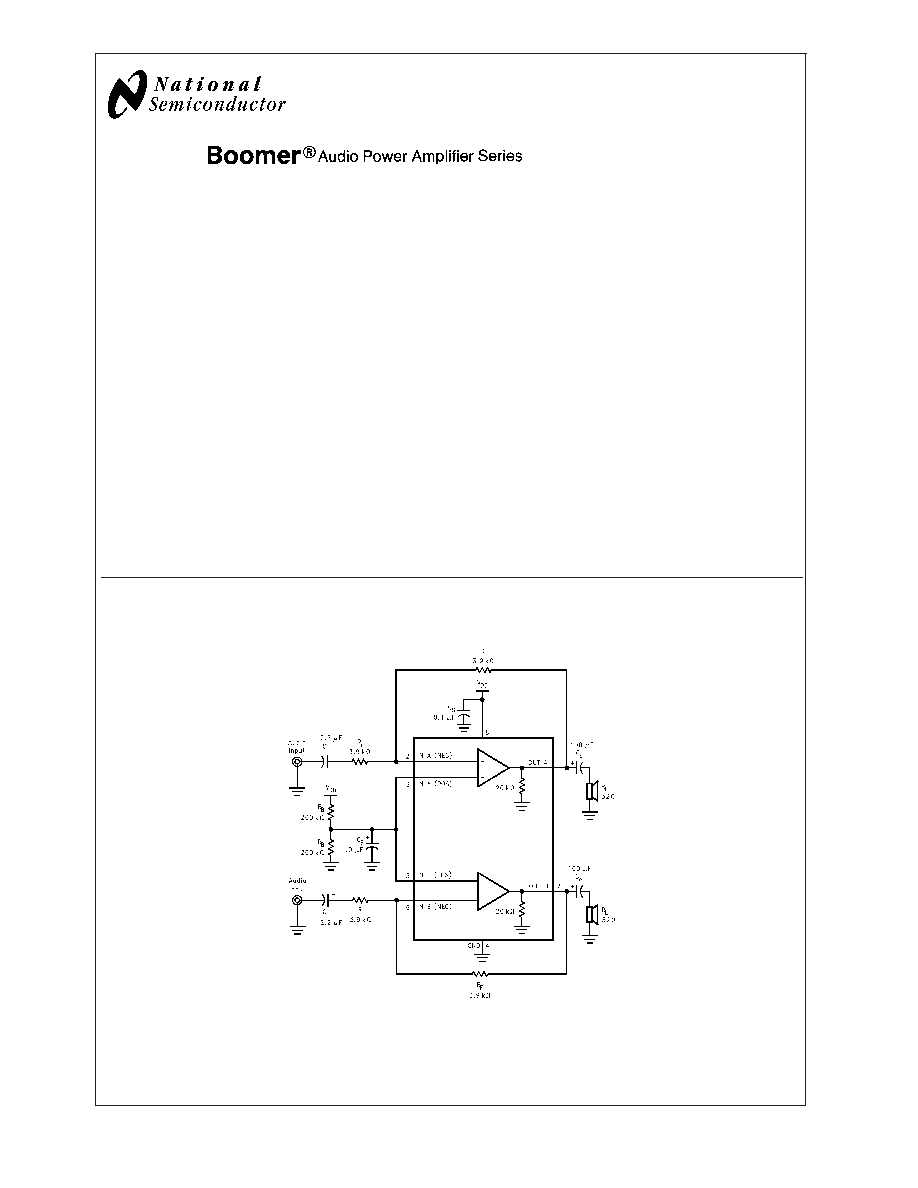
Typical Application
Boomer
�
is a registered trademark of National Semiconductor Corporation.
20075201
*Refer to the Application Information Section for information concerning proper selection of the input and output coupling capacitors.
FIGURE 1. Typical Audio Amplifier Application Circuit
February 2004
10kV
ESD
Rated,
Dual
120
mW
Headphone
Amplifier
� 2004 National Semiconductor Corporation
DS200752
www.national.com
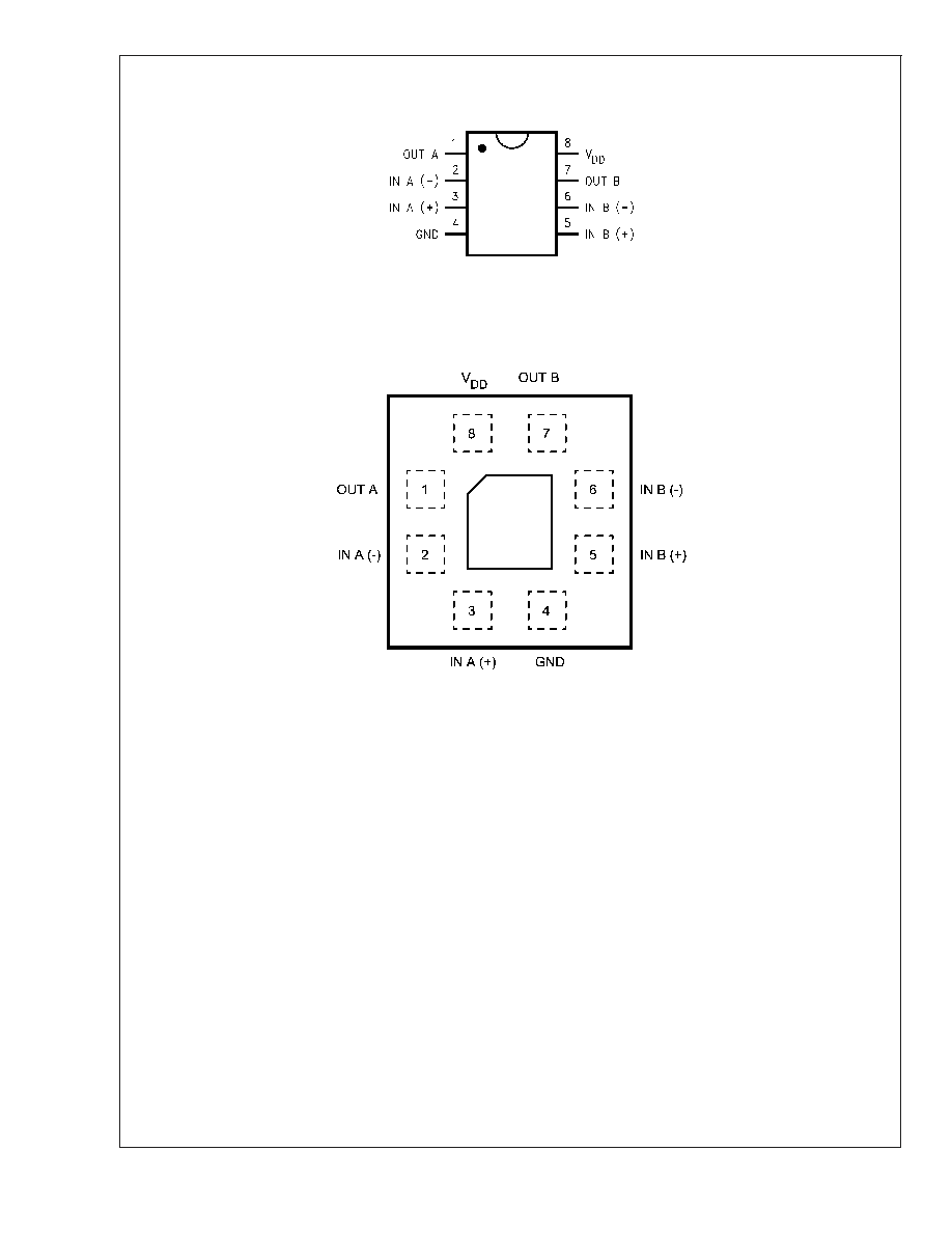
Connection Diagrams
SOP (MA) and MSOP (MM) Package
20075202
Top View
Order Number LM4908MA, LM4908MM
See NS Package Number M08A, MUA08A
LLP (LQ) Package
200752A2
Top View
Order Number LM4908LQ
See NS Package Number LQB08A
LM4908
www.national.com
2
Absolute Maximum Ratings
(Note 3)
If Military/Aerospace specified devices are required,
please contact the National Semiconductor Sales Office/
Distributors for availability and specifications.
Supply Voltage
6.0V
Storage Temperature
-65�C to +150�C
Input Voltage
-0.3V to V
DD
+ 0.3V
Power Dissipation (Note 4)
Internally limited
ESD Susceptibility (Note 5)
10.0kV
ESD Susceptibility (Note 6)
500V
Junction Temperature
150�C
Soldering Information (Note 1)
Small Outline Package
Vapor Phase (60 seconds)
215�C
Infrared (15 seconds)
220�C
Thermal Resistance
JC
(MSOP)
56�C/W
JA
(MSOP)
210�C/W
JC
(SOP)
35�C/W
JA
(SOP)
170�C/W
JC
(LLP)
15�C/W
JA
(LLP)
117�C/W (Note 9)
JA
(LLP)
150�C/W (Note 10)
Operating Ratings
Temperature Range
T
MIN
T
A
T
MAX
-40�C
T
A
85�C
Supply Voltage
2.0V
V
DD
5.5V
Note 1: See AN-450 "Surface Mounting and their Effects on Product Reli-
ability" for other methods of soldering surface mount devices.
Electrical Characteristics
(Notes 2, 3)
The following specifications apply for V
DD
= 5V unless otherwise specified, limits apply to T
A
= 25�C.
Symbol
Parameter
Conditions
LM4908
Units
(Limits)
Typ
(Note 7)
Limit
(Note 8)
V
DD
Supply Voltage
2.0
V (min)
5.5
V (max)
I
DD
Supply Current
V
IN
= 0V, I
O
= 0A
1.6
3.0
mA (max)
P
tot
Total Power Dissipation
V
IN
= 0V, I
O
= 0A
8
16.5
mW (max)
V
OS
Input Offset Voltage
V
IN
= 0V
5
50
mV (max)
Ibias
Input Bias Current
10
pA
V
CM
Common Mode Voltage
0
V
4.3
V
G
V
Open-Loop Voltage Gain
R
L
= 5k
67
dB
Io
Max Output Current
THD+N
<
0.1 %
70
mA
R
O
Output Resistance
0.1
V
O
Output Swing
R
L
= 32
, 0.1% THD+N, Min
.3
V
R
L
= 32
, 0.1% THD+N, Max
4.7
PSRR
Power Supply Rejection Ratio
Cb = 1.0�F, Vripple = 100mV
PP
,
f = 40Hz
90
dB
Crosstalk
Channel Separation
R
L
= 32
, f = 1kHz
82
dB
THD+N
Total Harmonic Distortion + Noise
f = 1 kHz
R
L
= 16
,
V
O
=3.5V
PP
(at 0 dB)
0.05
%
66
dB
R
L
= 32
,
V
O
=3.5V
PP
(at 0 dB)
0.05
%
66
dB
SNR
Signal-to-Noise Ratio
V
O
= 3.5V
pp
(at 0 dB)
100
dB
f
G
Unity Gain Frequency
Open Loop, R
L
= 5k
25
MHz
P
o
Output Power
THD+N = 0.1%, f = 1 kHz
R
L
= 16
120
mW
R
L
= 32
75
60
mW
THD+N = 10%, f = 1 kHz
R
L
= 16
157
mW
R
L
= 32
99
mW
C
I
Input Capacitance
3
pF
LM4908
www.national.com
3
Electrical Characteristics
(Notes 2, 3) (Continued)
The following specifications apply for V
DD
= 5V unless otherwise specified, limits apply to T
A
= 25�C.
Symbol
Parameter
Conditions
LM4908
Units
(Limits)
Typ
(Note 7)
Limit
(Note 8)
C
L
Load Capacitance
200
pF
SR
Slew Rate
Unity Gain Inverting
3
V/�s
Electrical Characteristics
(Notes 2, 3)
The following specifications apply for V
DD
= 3.3V unless otherwise specified, limits apply to T
A
= 25�C.
Symbol
Parameter
Conditions
Conditions
Units
(Limits)
Typ
(Note 7)
Limit
(Note 8)
I
DD
Supply Current
V
IN
= 0V, I
O
= 0A
1.4
mA (max)
V
OS
Input Offset Voltage
V
IN
= 0V
5
mV (max)
P
o
Output Power
THD+N = 0.1%, f = 1 kHz
R
L
= 16
43
mW
R
L
= 32
30
mW
THD+N = 10%, f = 1 kHz
R
L
= 16
61
mW
R
L
= 32
41
mW
Electrical Characteristics
(Notes 2, 3)
The following specifications apply for V
DD
= 2.6V unless otherwise specified, limits apply to T
A
= 25�C.
Symbol
Parameter
Conditions
Conditions
Units
(Limits)
Typ
(Note 7)
Limit
(Note 8)
I
DD
Supply Current
V
IN
= 0V, I
O
= 0A
1.3
mA (max)
V
OS
Input Offset Voltage
V
IN
= 0V
5
mV (max)
P
o
Output Power
THD+N = 0.1%, f = 1 kHz
R
L
= 16
20
mW
R
L
= 32
16
mW
THD+N = 10%, f = 1 kHz
R
L
= 16
34
mW
R
L
= 32
24
mW
Note 2: All voltages are measured with respect to the ground pin, unless otherwise specified.
Note 3: Absolute Maximum Ratings indicate limits beyond which damage to the device may occur. Operating Ratings indicate conditions for which the device is
functional, but do not guarantee specific performance limits. Electrical Characteristics state DC and AC electrical specifications under particular test conditions which
guarantee specific performance limits. This assumes that the device is within the Operating Ratings. Specifications are not guaranteed for parameters where no limit
is given, however, the typical value is a good indication of device performance.
Note 4: The maximum power dissipation must be derated at elevated temperatures and is dictated by T
JMAX
,
JA
, and the ambient temperature T
A
. The maximum
allowable power dissipation is P
DMAX
= (T
JMAX
- T
A
) /
JA
. For the LM4908, T
JMAX
= 150�C, and the typical junction-to-ambient thermal resistance, when board
mounted, is 210�C/W for package MUA08A and 170�C/W for package M08A.
Note 5: Human body model, 100pF discharged through a 1.5k
resistor.
Note 6: Machine Model, 220pF�240pF discharged through all pins.
Note 7: Typicals are measured at 25�C and represent the parametric norm.
Note 8: Tested limits are guaranteed to National's AOQL (Average Outgoing Quality Level). Datasheet min/max specification limits are guaranteed by design, test,
or statistical analysis.
Note 9: The given
JA
is for an LM4908 packaged in an LQB08A with the Exposed-DAP soldered to a printed circuit board copper pad with an area equivalent to
that of the Exposed-DAP itself.
Note 10: The given
JA
is for an LM4908 packaged in an LQB08A with the Exposed-DAP not soldered to any printed circuit board copper.
LM4908
www.national.com
4

External Components Description
(Figure 1)
Components
Functional Description
1. R
i
The inverting input resistance, along with R
f
, set the closed-loop gain. R
i
, along with C
i
, form a high
pass filter with f
c
= 1/(2
R
i
C
i
).
2. C
i
The input coupling capacitor blocks DC voltage at the amplifier's input terminals. C
i
, along with R
i
,
create a highpass filter with f
C
= 1/(2
R
i
C
i
). Refer to the section, Selecting Proper External
Components, for an explanation of determining the value of C
i
.
3. R
f
The feedback resistance, along with R
i
, set closed-loop gain.
4. C
S
This is the supply bypass capacitor. It provides power supply filtering. Refer to the Application
Information section for proper placement and selection of the supply bypass capacitor.
5. C
B
This is the half-supply bypass pin capacitor. It provides half-supply filtering. Refer to the section,
Selecting Proper External Components, for information concerning proper placement and selection
of C
B
.
6. C
O
This is the output coupling capacitor. It blocks the DC voltage at the amplifier's output and forms a high
pass filter with R
L
at f
O
= 1/(2
R
L
C
O
)
7. R
B
This is the resistor which forms a voltage divider that provides 1/2 V
DD
to the non-inverting input of the
amplifier.
Typical Performance
Characteristics
THD+N vs Frequency
V
DD
= 2.6V, PWR = 15mW, R
L
= 8
THD+N vs Frequency
V
DD
= 2.6V, PWR = 15mW, R
L
= 16
20075267
20075268
LM4908
www.national.com
5
Document Outline