 | –≠–ª–µ–∫—Ç—Ä–æ–Ω–Ω—ã–π –∫–æ–º–ø–æ–Ω–µ–Ω—Ç: LM6588 | –°–∫–∞—á–∞—Ç—å:  PDF PDF  ZIP ZIP |

LM6588
TFT-LCD Quad, 16V RRIO High Output Current
Operational Amplifier
General Description
The LM6588 is a low power, high voltage, rail-to-rail input-
output amplifier ideally suited for LCD panel V
COM
driver and
gamma buffer applications. The LM6588 contains four unity
gain stable amplifiers in one package. It provides a common
mode input ability of 0.5V beyond the supply rails, as well as
an output voltage range that extends to within 50mV of either
supply rail. With these capabilities, the LM6588 provides
maximum dynamic range at any supply voltage. Operating
on supplies ranging from 5V to 16V, while consuming only
750µA per amplifier, the LM6588 has a bandwidth of 24MHz
(-3dB).
The LM6588 also features fast slewing and settling times,
along with a high continuous output capability of 75mA. This
output stage is capable of delivering approximately 200mA
peak currents in order to charge or discharge capacitive
loads. These features are ideal for use in TFT-LCDs.
The LM6588 is available in the industry standard 14-pin SO
package and in the space-saving 14-pin TSSOP package.
The amplifiers are specified for operation over the full -40∞C
to +85∞C temperature range.
Features
(V
S
= 5V, T
A
= 25∞C typical values unless specified)
n
Input common mode voltage
0.5V beyond rails
n
Output voltage swing (R
L
= 2k
)
50mV from rails
n
Output short circuit current
±
200mA
n
Continuous output current
75mA
n
Supply current (per amp, no load)
750µA
n
Supply voltage range
5V to 16V
n
Unity gain stable
n
-3dB bandwidth (A
V
= +1)
24MHz
n
Slew rate
11V/µSec
n
Settling time
270ns
n
SO-14 and TSSOP-14 package
n
Manufactured in National Semiconductor's
state-of-the-art bonded wafer, trench isolated
complementary bipolar VIP10
TM
technology for high
performance at low power levels
Applications
n
LCD panel V
COM
driver
n
LCD panel gamma buffer
n
LCD panel repair amp
Test Circuit Diagram
20073401
May 2003
LM6588
TFT
-LCD
Quad,
16V
RRIO
High
Output
Current
Operational
Amplifier
© 2003 National Semiconductor Corporation
DS200734
www.national.com
Absolute Maximum Ratings
(Note 1)
If Military/Aerospace specified devices are required,
please contact the National Semiconductor Sales Office/
Distributors for availability and specifications.
ESD Tolerance (Note 2)
Human Body Model
2.5KV
Machine Model
250V
Supply Voltage (V
+
- V
-
)
18V
Differential Input Voltage
±
5.5V
Output Short Circuit to Ground (Note 3)
Continuous
Storage Temperature Range
-65∞C to 150∞C
Input Common Mode Voltage
V
-
to V
+
Junction Temperature (Note 4)
150∞C
Operating Ratings
(Note 1)
Supply Voltage
5V
V
S
16V
Temperature Range
-40∞C to +85∞C
Thermal Resistance (
JA
)
SOIC-14
145∞C/W
TSSOP-14
155∞C/W
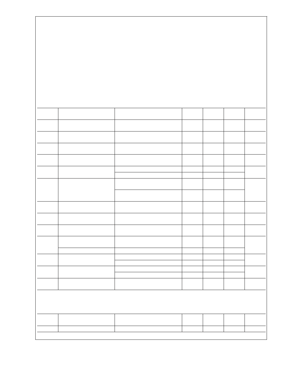
16V DC Electrical Characteristics
(Note 13)
Unless otherwise specified, all limits guaranteed for at T
J
= 25∞C, V
CM
=
1
/
2
V
S
and R
L
= 2k
. Boldface limits apply at the tem-
perature extremes.
Symbol
Parameter
Conditions
Min
(Note 6)
Typ
(Note 5)
Max
(Note 6)
Units
V
OS
Input Offset Voltage
0.7
4
6
mV
TC V
OS
Input Offset Voltage Average
Drift
5
µV/∞C
I
B
Input Bias Current
-0.3/+0.3
±
1
±
7
µA
I
OS
Input Offset Current
16
150
300
nA
R
IN
Input Resistance
Common Mode
20
M
Differential Mode
0.5
CMRR
Common Mode Rejection
Ratio
V
CM
= 0 to +16V
75
70
103
dB
V
CM
= 0 to 14.5V
78
72
103
PSRR
Power Supply Rejection Ratio
V
CM
=
±
1V
80
75
103
dB
CMVR
Input Common-Mode Voltage
Range
CMRR
>
50dB
16.2
0
16
-0.2
V
A
V
Large Signal Voltage Gain
(Note 7)
R
L
= 2k
, V
O
= 0.5 to +15.5V
80
75
108
dB
V
O
Output Swing High
R
L
= 2k
15.8
15.6
15.9
V
Output Swing Low
R
L
= 2k
0.100
0.200
I
SC
Output Short Circuit Current
(Note 11)
Sourcing
170
230
mA
Sinking
170
230
I
CONT
Continuous Output Current
(Note 12)
Sourcing
40
mA
Sinking
40
I
S
Supply Current (per Amp)
800
1200
1500
µA
16V AC Electrical Characteristics
(Note 13)
Unless otherwise specified, all limits guaranteed for at T
J
= 25∞C, V
CM
=
1
/
2
V
S
and R
L
= 2k
. Boldface limits apply at the tem-
perature extremes.
Symbol
Parameter
Conditions
Min
(Note 6)
Typ
(Note 5)
Max
(Note 6)
Units
SR
Slew Rate (Note 9)
A
V
= +1, V
IN
= 10V
PP
8
15
V/µs
LM6588
www.national.com
2

16V AC Electrical Characteristics
(Note 13) (Continued)
Unless otherwise specified, all limits guaranteed for at T
J
= 25∞C, V
CM
=
1
/
2
V
S
and R
L
= 2k
. Boldface limits apply at the tem-
perature extremes.
Symbol
Parameter
Conditions
Min
(Note 6)
Typ
(Note 5)
Max
(Note 6)
Units
Unity Gain Bandwidth Product
15.4
MHz
-3dB Frequency
A
V
= +1
10
24
MHz
m
Phase Margin
61
deg
t
s
Settling Time (0.1%)
A
V
= -1, A
O
=
±
5V, R
L
= 500
780
ns
t
p
Propagation Delay
A
V
= -2, V
IN
=
±
5V, R
L
= 500
20
ns
HD2
2
nd
Harmonic Distortion
F
IN
= 1MHz (Note 10)
V
OUT
= 2V
PP
-53
dBc
HD3
3rd Harmonic Distortion
F
IN
= 1MHz (Note 10)
V
OUT
= 2V
PP
-40
dBc
e
n
Input-Referred Voltage Noise
f = 10kHz
23
nV/
5V DC Electrical Characteristics
(Note 13)
Unless otherwise specified, all limits guaranteed for at T
J
= 25∞C, V
CM
=
1
/
2
V
S
and R
L
= 2k
. Boldface limits apply at the tem-
perature extremes.
Symbol
Parameter
Conditions
Min
(Note 6)
Typ
(Note 5)
Max
(Note 6)
Units
V
OS
Input Offset Voltage
0.7
4
6
mV
TC V
OS
Input Offset Voltage Average
Drift
10
µV/∞C
I
B
Input Bias Current
-0.3/+0.3
±
1
±
7
µA
I
OS
Input Offset Current
20
150
300
nA
R
IN
Input Resistance
Common Mode
20
M
Differential Mode
0.5
CMRR
Common Mode Rejection
Ratio
V
CM
Stepped from 0 to 5V
70
66
105
dB
V
CM
Stepped from 0 to 3.5V
75
70
105
PSRR
Power Supply Rejection Ratio
V
S
= V
CC
= 3.5V to 5.5V
80
75
92
dB
CMVR
Input Common-Mode Voltage
Range
CMRR
>
50dB
5.2
0.0
5.0
-0.2
V
A
V
Large Signal Voltage Gain
(Note 7)
R
L
= 2k
, V
O
= 0 to 5V
80
75
106
dB
V
O
Output Swing High
R
L
= 2k
4.85
4.7
4.95
V
Output Swing Low
R
L
= 2k
0.05
0.15
I
SC
Output Short Circuit Current
(Note 11)
Sourcing
160
200
mA
Sinking
160
200
I
CONT
Continuous Output Current
(Note 12)
Sourcing
75
mA
Sinking
75
I
S
Supply Current (per Amp)
750
1000
1250
µA
LM6588
www.national.com
3

5V AC Electrical Characteristics
(Note 13)
Unless otherwise specified, all limits guaranteed for at T
J
= 25∞C, V
CM
=
1
/
2
V
S
and R
L
= 2k
. Boldface limits apply at the tem-
perature extremes.
Symbol
Parameter
Conditions
Min
(Note 6)
Typ
(Note 5)
Max
(Note 6)
Units
SR
Slew Rate (Note 9)
A
V
= +1, V
IN
= 3.5V
PP
11
V/µs
Unity Gain Bandwidth Product
15.3
MHz
-3dB Frequency
A
V
= +1
10
24
MHz
m
Phase Margin
56
deg
t
s
Settling Time (0.1%)
A
V
= -1, V
O
=
±
1V, R
L
= 500
270
ns
t
p
Propagation Delay
A
V
= -2, V
IN
=
±
1V, R
L
= 500
21
ns
HD2
2
nd
Harmonic Distortion
F
IN
= 1MHz (Note 10)
V
OUT
= 2V
PP
-53
dBc
HD3
3rd Harmonic Distortion
F
IN
= 1MHz (Note 10)
V
OUT
= 2V
PP
-40
dBc
e
n
Input-Referred Voltage Noise
f = 10kHz
23
nV/
Note 1: Note 1: Absolute maximum Ratings indicate limits beyond which damage to the device may occur. Operating Ratings indicate conditions for which the
device is intended to be functional, but specific performance is not guaranteed. For guaranteed specifications and the test conditions, see the Electrical
Characteristics.
Note 2: For testing purposes, ESD was applied using human body model, 1.5k
in series with 100pF.
Note 3: Applies to both single-supply and split-supply operation. Continuous short circuit operation at elevated ambient temperature can result in exceeding the
maximum allowed junction temperature of 150∞C
Note 4: The maximum power dissipation is a function of T
J(MAX)
,
JA
, and T
A
. The maximum allowable power dissipation at any ambient temperature is
P
D
= (T
J(MAX)
- T
A
)/
JA
. All numbers apply for packages soldered directly onto a PC board.
Note 5: Typical values represent the most likely parametric norm.
Note 6: All limits are guaranteed by testing or statistical analysis.
Note 7: Large signal voltage gain is the total output swing divided by the input signal required to produce that swing.
Note 8: The open loop output current is guaranteed, by the measurement of the open loop output voltage swing.
Note 9: Slew rate is the average of the raising and falling slew rates.
Note 10: Harmonics are measured with A
V
= +2 and R
L
= 100
and V
IN
= 1V
PP
to give V
OUT
= 2V
PP
.
Note 11: Continuous operation at these output currents will exceed the power dissipation ability of the device
Note 12: Power dissipation limits may be exceeded if all four amplifiers source or sink 40mA. Voltage across the output transistors and their output currents must
be taken into account to determine the power dissipation of the device
Note 13: Electrical table values apply only for factory testing conditions at the temperature indicated. Factory testing conditions result in very limited self-heating of
the device such that T
J
= T
A
. No guarantee of parametric performance is indicated in the electrical tables under conditions of internal self heating where T
J
>
T
A
.
See applications section for information on temperature de-rating of this device.
Connection Diagram
14-Pin SOIC/TSSOP
20073402
Top View
Ordering Information
Package
Part Number
Package Marking
Transport Media
NSC Drawing
14-Pin SOIC
LM6588MA
LM6588MA
95 Units/Rail
M14A
LM6588MAX
2.5k Units Tape and Reel
14-Pin TSSOP
LM6588MT
LM6588MT
95 Units/Rail
MTC14
LM6588MTX
2.5k Units Tape and Reel
LM6588
www.national.com
4

Typical Performance Characteristics
Unless otherwise specified, all limits guaranteed for T
J
= 25∞C,
V
CM
= 1/2V
S
and R
L
= 2k
.
Gain Phase vs. Temperature (V
S
= 5V)
Gain Phase vs. Temperature (V
S
= 16V)
20073403
20073404
Gain Phase vs. Capacitive Loading (V
S
= 5V)
Gain Phase vs. Capacitive Loading (V
S
= 16V)
20073405
20073406
PSRR (V
S
= 5V)
PSRR (V
S
= 16V)
20073407
20073408
LM6588
www.national.com
5