LM70
SPI/MICROWIRE
TM
10-Bit plus Sign Digital Temperature
Sensor
General Description
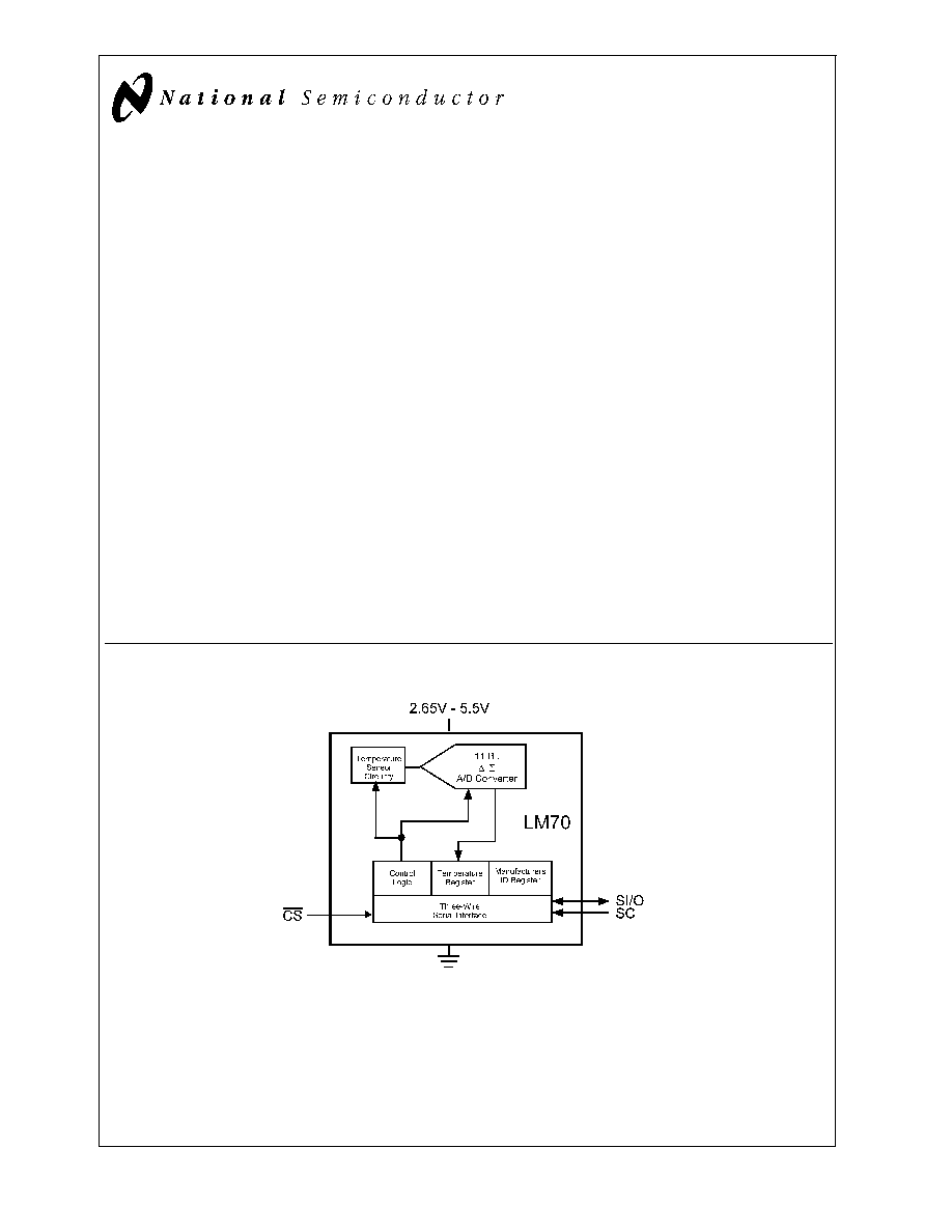
The
LM70
is
a
temperature
sensor,
Delta-Sigma
analog-to-digital converter with an SPI and MICROWIRE
compatible interface available in LLP and MSOP 8-pin pack-
ages. The host can query the LM70 at any time to read tem-
perature. A shutdown mode decreases power consumption
to less than 10 µA. This mode is useful in systems where low
average power consumption is critical.
The LM70 has 10-bit plus sign temperature resolution
(0.25∞C per LSB) while operating over a temperature range
of -55∞C to +150∞C.
The LM70's 2.65V to 5.5V supply voltage range, low supply
current and simple SPI interface make it ideal for a wide
range of applications. These include thermal management
and protection applications in hard disk drives, printers, elec-
tronic test equipment, and office electronics.
Applications
n
System Thermal Management
n
Personal Computers
n
Disk Drives
n
Office Electronics
n
Electronic Test Equipment
Features
n
0.25∞C temperature resolution.
n
Shutdown mode conserves power between temperature
reading
n
SPI and MICROWIRE Bus interface
n
MSOP-8 and LLP-8 packages save space
Key Specifications
j
Supply Voltage
2.65V to 5.5V
j
Supply Current
operating
260µA (typ)
490µA (max)
shutdown
12µA (typ)
j
Temperature
Accuracy
-40∞C to 85∞C
±
2∞C(max)
-10∞C to 65∞C
+1.5/-2∞C(max)
-55∞C to 125∞C
+3/-2∞C(max)
-55∞C to 150∞C
+3.5/-2∞C(max)
Simplified Block Diagram
MICROWIRE
Æ
is a registered trademark of National Semiconductor Corporation.
DS101223-1
July 2000
LM70
SPI/MICROWIRE10-Bit
plus
Sign
Digital
T
emperature
Sensor
© 2000 National Semiconductor Corporation
DS101223
www.national.com
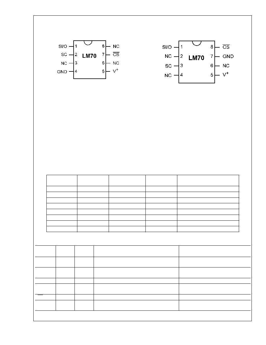
Connection Diagrams
Ordering Information
Order Number
Package
Marking
NS Package
Number
Supply Voltage
Transport Media
LM70CILD-3
T33
LLP-8, LDA08A
2.65V to 3.6V
_ Units in Rail
LM70CILDX-3
T33
LLP-8, LDA08A
2.65V to 3.6V
_ Units in Rail
LM70CILD-5
T35
LLP-8, LDA08A
4.5V to 5.5V
_ Units in Tape and Reel
LM70CILDX-5
T35
LLP-8, LDA08A
4.5V to 5.5V
_ Units in Tape and Reel
LM70CIMM-3
T04C
MSOP-8, MUA08A
2.65V to 3.6V
250 Units in Rail
LM70CIMMX-3
T04C
MSOP-8, MUA08A
2.65V to 3.6V
3500 Units in Tape and Reel
LM70CIMM-5
T03C
MSOP-8, MUA08A
4.5V to 5.5V
250 Units in Rail
LM70CIMMX-5
T03C
MSOP-8, MUA08A
4.5V to 5.5V
3500 Units in Tape and Reel
Pin Descriptions
Label
SOP-8
Pin #
LLP-8
Pin #
Function
Typical Connection
SI/O
1
1
Input/Output - Serial bus bi-directional data
line. Schmitt trigger input.
From and to Controller
SC
2
3
Clock - Serial bus clock Schmitt trigger input
line.
From Controller
GND
4
7
Power Supply Ground
Ground
V
+
5
5
Positive Supply Voltage Input
DC Voltage from 2.65V to 5.5V. Bypass
with a 0.1 µF ceramic capacitor.
CS
7
8
Chip Select input.
From Controller
NC
3, 6, 8
2, 4, 6
No Connect
These pins are not connected to the
LM70 die in any way.
MSOP-8
DS101223-2
TOP VIEW
NS Package Number MUA08A
LLP-8
DS101223-25
TOP VIEW
NS Package Number LDA08A
LM70
www.national.com
2
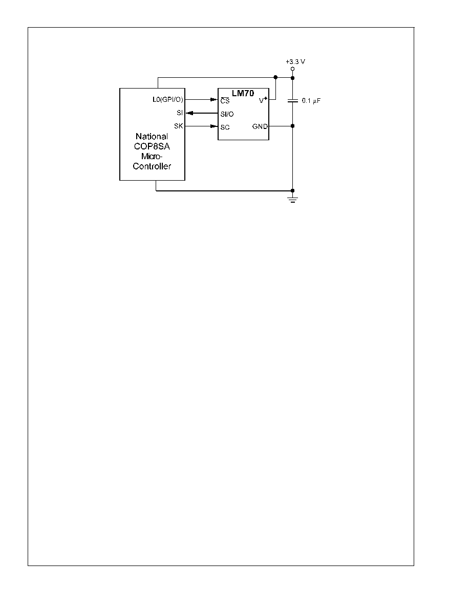
Typical Application
DS101223-3
FIGURE 1. COP Microcontroller Interface
LM70
www.national.com
3

Absolute Maximum Ratings
(Note 1)
Supply Voltage
-0.3V to 6.0V
Voltage at any Pin
-0.3V to V
+
+ 0.3V
Input Current at any Pin (Note 2)
5 mA
Package Input Current (Note 2)
20 mA
Storage Temperature
-65∞C to +150∞C
Soldering Information, Lead Temperature
MSOP-8 and LLP-8 Packages
(Note 3)
Vapor Phase (60 seconds)
Infrared (15 seconds)
215∞C
220∞C
ESD Susceptibility (Note 4)
Human Body Model
3000V
Machine Model
300V
Operating Ratings
Specified Temperature Range
T
MIN
to T
MAX
(Note 5)
-55∞C to +150∞C
Supply Voltage Range (+V
S
)
+2.65V to +5.5V
Temperature-to-Digital Converter Characteristics
Unless otherwise noted, these specifications apply for V
+
= 2.65V to 3.6V for the LM70-3 and V
+
= 4.5V to 5.5V for the LM70-5
(Note 6). Boldface limits apply for T
A
= T
J
= T
MIN
to T
MAX
; all other limits T
A
= T
J
=+25∞C, unless otherwise noted.
Parameter
Conditions
Typical
(Note 7)
LM70-5
Limits
(Note 8)
LM70-3
Limits
(Note 8)
Units
(Limit)
Temperature Error (Note 6)
T
A
= -10∞C to +65∞C
+1.5/-2.0
+1.5/-2.0
∞C (max)
T
A
= -40∞C to +85∞C
±
2.0
±
2.0
∞C (max)
T
A
= -55∞C to +125∞C
+3.0/-2.0
+3.0/-2.0
∞C (max)
T
A
= -55∞C to +150∞C
+3.5/-2.0
+3.5/-2.0
∞C (max)
Resolution
11
0.25
Bits
∞C
Temperature Conversion Time
(Note 9)
140
210
210
ms (max)
Quiescent Current
Serial Bus Inactive
260
490
490
µA (max)
Serial Bus Active
260
µA
Shutdown Mode
12
µA
Logic Electrical Characteristics
DIGITAL DC CHARACTERISTICS
Unless otherwise noted, these specifications apply for V
+
= 2.65V to 3.6V for the LM70-3 and V
+
= 4.5V to 5.5V for the
LM70-5. Boldface limits apply for T
A
= T
J
= T
MIN
to T
MAX
; all other limits T
A
= T
J
=+25∞C, unless otherwise noted.
Symbol
Parameter
Conditions
Typical
(Note 7)
Limits
(Note 8)
Units
(Limit)
V
IN(1)
Logical "1" Input Voltage
V
+
x 0.7
V (min)
V
+
+ 0.3
V (max)
V
IN(0)
Logical "0" Input Voltage
-0.3
V (min)
V
+
x 0.3
V (max)
Input Hysteresis Voltage
V
+
= 2.65V to 3.6V
0.8
0.27
V (min)
V
+
= 4.5V to 5.5V
0.8
0.35
V (min)
I
IN(1)
Logical "1" Input Current
V
IN
= V
+
0.005
3.0
µA (max)
I
IN(0)
Logical "0" Input Current
V
IN
= 0V
-0.005
-3.0
µA (min)
C
IN
All Digital Inputs
20
pF
V
OH
High Level Output Voltage
I
OH
= -400 µA
2.4
V (min)
V
OL
Low Level Output Voltage
I
OL
= +2 mA
0.4
V (max)
I
O_TRI-STATE
TRI-STATE Output Leakage
Current
V
O
= GND
V
O
= V
+
-1
+1
µA (min)
µA(max)
LM70
www.national.com
4
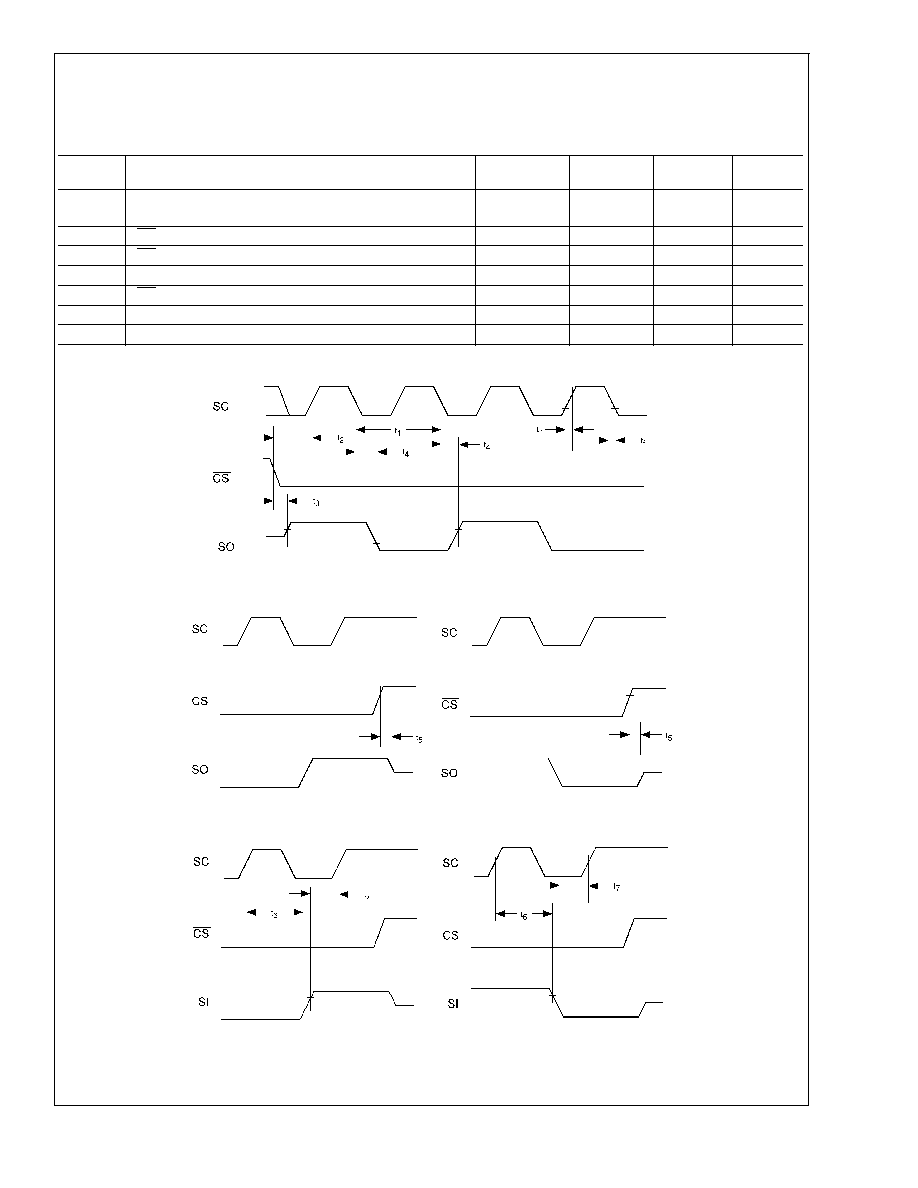
Logic Electrical Characteristics
(Continued)
SERIAL BUS DIGITAL SWITCHING CHARACTERISTICS
Unless otherwise noted, these specifications apply for V
+
= 2.65V to 3.6V for the LM70-3 and V
+
= 4.5V to 5.5V for the
LM70-5, C
L
(load capacitance) on output lines = 100 pF unless otherwise specified. Boldface limits apply for T
A
= T
J
=
T
MIN
to T
MAX
; all other limits T
A
= T
J
= +25∞C, unless otherwise noted.
Symbol
Parameter
Conditions
Typical
(Note 7)
Limits
(Note 8)
Units
(Limit)
t
1
SC (Clock) Period
0.16
DC
µs (min)
(max)
t
2
CS Low to SC (Clock) High Set-Up Time
100
ns (max)
t
3
CS Low to Data Out (SO) Delay
70
ns (max)
t
4
SC (Clock) Low to Data Out (SO) Delay
70
ns (max)
t
5
CS High to Data Out (SO) TRI-STATE
200
ns (min)
t
6
SC (Clock) High to Data In (SI) Hold Time
60
ns (min)
t
7
Data In (SI) Set-Up Time to SC (Clock) High
30
ns (min)
DS101223-4
FIGURE 2. Data Output Timing Diagram
DS101223-5
FIGURE 3. TRI-STATE Data Output Timing Diagram
DS101223-6
FIGURE 4. Data Input Timing Diagram
LM70
www.national.com
5