 | –≠–ª–µ–∫—Ç—Ä–æ–Ω–Ω—ã–π –∫–æ–º–ø–æ–Ω–µ–Ω—Ç: LM7121IN | –°–∫–∞—á–∞—Ç—å:  PDF PDF  ZIP ZIP |

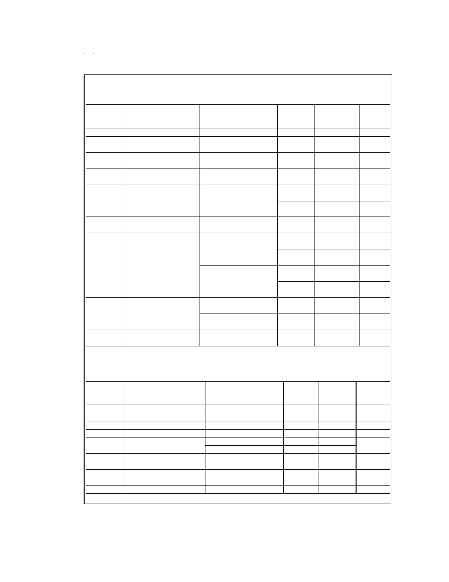
LM7121
235 MHz Tiny Low Power Voltage Feedback Amplifier
General Description
The LM7121 is a high performance operational amplifier
which addresses the increasing AC performance needs of
video and imaging applications, and the size and power con-
straints of portable applications.
The LM7121 can operate over a wide dynamic range of sup-
ply voltages, from 5V (single supply) up to
±
15V (see the Ap-
plication Information section for more details). It offers an ex-
cellent speed-power product delivering 1300V/µs and 235
MHz Bandwidth (-3 dB, A
V
= +1). Another key feature of this
operational amplifier is stability while driving unlimited ca-
pacitive loads.
Due to its Tiny SOT23-5 package, the LM7121 is ideal for
designs where space and weight are the critical parameters.
The benefits of the Tiny package are evident in small por-
table electronic devices, such as cameras, and PC video
cards. Tiny amplifiers are so small that they can be placed
anywhere on a board close to the signal source or near the
input to an A/D converter.
Features
(Typical unless otherwise noted) V
S
=
±
15V
n
Easy to use voltage feedback topology
n
Stable with unlimited capacitive loads
n
Tiny SOT23-5 package -- typical circuit layout takes half
the space of SO-8 designs
n
Unity gain frequency:
175 MHz
n
Bandwidth (-3 dB, A
V
= +1, R
L
= 100
):
235 MHz
n
Slew rate:
1300V/µs
n
Supply Voltages SO-8:
5V to
±
15V
SOT23-5:
5V to
±
5V
n
Characterized for:
+5V,
±
5V,
±
15V
n
Low supply current:
5.3 mA
Applications
n
Scanners, color fax, digital copiers
n
PC video cards
n
Cable drivers
n
Digital cameras
n
ADC/DAC buffers
n
Set-top boxes
Connection Diagrams
Ordering Information
Package
Ordering Information
NSC Drawing
Package
Supplied As
Number
Marking
8-Pin SO-8
LM7121IM
M08A
LM7121IM
Rails
LM7121IMX
M08A
LM7121IM
2.5k Tape and Reel
5-Pin SOT23-5
LM7121IM5
MA05A
A03A
1k Tape and Reel
LM7121IM5X
MA05A
A03A
3k Tape and Reel
8-Pin SO-8
DS012348-2
Top View
5-Pin SOT23
DS012348-1
Top View
August 1999
LM7121
235
MHz
T
iny
Low
Power
V
oltage
Feedback
Amplifier
© 1999 National Semiconductor Corporation
DS012348
www.national.com

Absolute Maximum Ratings
(Note 1)
If Military/Aerospace specified devices are required,
please contact the National Semiconductor Sales Office/
Distributors for availability and specifications.
ESD Tolerance (Note 2)
2000V
Differential Input Voltage (Note 7)
±
2V
Voltage at Input/Output Pin
(V
+
)-1.4V, (V
-
)+1.4V
Supply Voltage (V
+
≠V
-
)
36V
Output Short Circuit to Ground
(Note 3)
Continuous
Lead Temperature
260∞C
(soldering, 10 sec)
260∞C
Storage Temperature Range
-65∞C to +150∞C
Junction Temperature (Note 4)
150∞C
Operating Ratings
(Note 1)
Supply Voltage: SO-8
4.5V
V
S
33V
SOT23-5
4.5V
V
S
11V
Junction Temperature Range
-40∞C
T
J
+85∞C
Thermal Resistance (
JA
)
M Package, 8-pin Surface Mount
165∞C/W
SOT23-5 Package
325∞C/W
±
15V DC Electrical Characteristics
Unless otherwise specified, all limits guaranteed for T
J
= 25∞C, V
+
= +15V, V
-
= -15V, V
CM
= V
O
= 0V and R
L
>
1 M
.
Boldface limits apply at the temperature extremes.
Symbol
Parameter
Conditions
Typ
(Note 5)
LM7121I
Units
Limit
(Note 6)
V
OS
Input Offset Voltage
0.9
8
mV
15
max
I
B
Input Bias Current
5.2
9.5
µA
12
max
I
OS
Input Offset Current
0.04
4.3
µA
7
max
R
IN
Input Resistance
Common Mode
10
M
Differential Mode
3.4
M
C
IN
Input Capacitance
Common Mode
2.3
pF
CMRR
Common Mode
-10V
V
CM
10V
93
73
dB
Rejection Ratio
70
min
+PSRR
Positive Power Supply
10V
V
+
15V
86
70
dB
Rejection Ratio
68
min
-PSRR
Negative Power Supply
-15V
V
-
-10V
81
68
dB
Rejection Ratio
65
min
V
CM
Input Common-Mode
CMRR
70 dB
13
11
V
Voltage Range
min
-13
-11
V
max
A
V
Large Signal
R
L
= 2 k
, V
O
= 20 V
PP
72
65
dB
Voltage Gain
57
min
V
O
Output Swing
R
L
= 2 k
13.4
11.1
V
10.8
min
-13.4
-11.2
V
-11.0
max
R
L
= 150
10.2
7.75
V
7.0
min
-7.0
-5.0
V
-4.8
max
I
SC
Output Short Circuit
Sourcing
71
54
mA
Current
44
min
Sinking
52
39
mA
34
min
www.national.com
2

±
15V DC Electrical Characteristics
(Continued)
Unless otherwise specified, all limits guaranteed for T
J
= 25∞C, V
+
= +15V, V
-
= -15V, V
CM
= V
O
= 0V and R
L
>
1 M
.
Boldface limits apply at the temperature extremes.
Symbol
Parameter
Conditions
Typ
(Note 5)
LM7121I
Units
Limit
(Note 6)
I
S
Supply Current
5.3
6.6
mA
7.5
max
±
15V AC Electrical Characteristics
Unless otherwise specified, all limits guaranteed for T
J
= 25∞C, V
+
= 15V, V
-
= -15V, V
CM
= V
O
= 0V and R
L
>
1 M
. Bold-
face limits apply at the temperature extremes.
Symbol
Parameter
Conditions
Typ
(Note 5)
LM7121I
Units
Limit
(Note 6)
SR
Slew Rate
A
V
= +2, R
L
= 1 k
,
1300
V/µs
(Note 8)
V
O
= 20 V
PP
GBW
Unity Gain-Bandwidth
R
L
= 1 k
175
MHz
m
Phase Margin
63
Deg
f (-3 dB)
Bandwidth
R
L
= 100
, A
V
= +1
235
MHz
(Notes 9, 10)
R
L
= 100
, A
V
= +2
50
t
s
Settling Time
10 V
PP
Step, to 0.1%,
74
ns
R
L
= 500
t
r
, t
f
Rise and Fall Time
A
V
= +2, R
L
= 100
,
5.3
ns
(Note 10)
V
O
= 0.4 V
PP
A
D
Differential Gain
A
V
= +2, R
L
= 150
0.3
%
D
Differential Phase
A
V
= +2, R
L
= 150
0.65
Deg
e
n
Input-Referred
f = 10 kHz
17
Voltage Noise
i
n
Input-Referred
f = 10 kHz
1.9
Current Noise
T.H.D.
Total Harmonic Distortion
2 V
PP
Output, R
L
= 150
,
0.065
%
A
V
= +2, f = 1 MHz
2 V
PP
Output, R
L
= 150
,
0.52
A
V
= +2, f = 5 MHz
±
5V DC Electrical Characteristics
Unless otherwise specified, all limits guaranteed for T
J
= 25∞C, V
+
= 5V, V
-
= -5V, V
CM
= V
O
= 0V and R
L
>
1 M
. Bold-
face limits apply at the temperature extremes.
Symbol
Parameter
Conditions
Typ
(Note 5)
LM7121I
Units
Limit
(Note 6)
V
OS
Input Offset Voltage
1.6
8
mV
15
max
I
B
Input Bias Current
5.5
9.5
µA
12
max
I
OS
Input Offset Current
0.07
4.3
µA
7.0
max
R
IN
Input Resistance
Common Mode
6.8
M
Differential Mode
3.4
M
www.national.com
3

±
5V DC Electrical Characteristics
(Continued)
Unless otherwise specified, all limits guaranteed for T
J
= 25∞C, V
+
= 5V, V
-
= -5V, V
CM
= V
O
= 0V and R
L
>
1 M
. Bold-
face limits apply at the temperature extremes.
Symbol
Parameter
Conditions
Typ
(Note 5)
LM7121I
Units
Limit
(Note 6)
C
IN
Input Capacitance
Common Mode
2.3
pF
CMRR
Common Mode
-2V
V
CM
2V
75
65
dB
Rejection Ratio
60
min
+PSRR
Positive Power Supply
3V
V
+
5V
89
65
dB
Rejection Ratio
60
min
-PSRR
Negative Power Supply
-5V
V
-
-3V
78
65
dB
Rejection Ratio
60
min
V
CM
Input Common Mode
CMRR
60 dB
3
2.5
V
Voltage Range
min
-3
-2.5
V
max
A
V
Large Signal
R
L
= 2 k
, V
O
= 3 V
PP
66
60
dB
Voltage Gain
58
min
V
O
Output Swing
R
L
= 2 k
3.62
3.0
V
2.75
min
-3.62
-3.0
V
-2.70
max
R
L
= 150
3.1
2.5
V
2.3
min
-2.8
-2.15
V
-2.00
max
I
SC
Output Short Circuit
Sourcing
53
38
mA
Current
33
min
Sinking
29
21
mA
19
min
I
S
Supply Current
5.1
6.4
mA
7.2
max
±
5V AC Electrical Characteristics
Unless otherwise specified, all limits guaranteed for T
J
= 25∞C, V
+
= 5V, V
-
= -5V, V
CM
= V
O
= 0V and R
L
>
1 M
. Bold-
face limits apply at the temperature extremes.
Symbol
Parameter
Conditions
Typ
(Note 5)
LM7121I
Units
Limit
(Note 6)
SR
Slew Rate
A
V
= +2, R
L
= 1 k
,
520
V/µs
(Note 8)
V
O
= 6 V
PP
GBW
Unity Gain-Bandwidth
R
L
= 1 k
105
MHz
m
Phase Margin
R
L
= 1 k
74
Deg
f (-3 dB)
Bandwidth
R
L
= 100
, A
V
= +1
160
MHz
(Notes 9, 10)
R
L
= 100
, A
V
= +2
50
t
s
Settling Time
5 V
PP
Step, to 0.1%,
65
ns
R
L
= 500
t
r
, t
f
Rise and Fall Time
A
V
= +2, R
L
= 100
,
5.8
ns
(Note 10)
V
O
= 0.4 V
PP
A
D
Differential Gain
A
V
= +2, R
L
= 150
0.3
%
www.national.com
4

±
5V AC Electrical Characteristics
(Continued)
Unless otherwise specified, all limits guaranteed for T
J
= 25∞C, V
+
= 5V, V
-
= -5V, V
CM
= V
O
= 0V and R
L
>
1 M
. Bold-
face limits apply at the temperature extremes.
Symbol
Parameter
Conditions
Typ
(Note 5)
LM7121I
Units
Limit
(Note 6)
D
Differential Phase
A
V
= +2, R
L
= 150
0.65
Deg
e
n
Input-Referred
f = 10 kHz
17
Voltage Noise
i
n
Input-Referred
f = 10 kHz
2
Current Noise
T.H.D.
Total Harmonic Distortion
2 V
PP
Output, R
L
= 150
,
0.1
%
A
V
= +2, f = 1 MHz
2 V
PP
Output, R
L
= 150
,
0.6
A
V
= +2, f = 5 MHz
+5V DC Electrical Characteristics
Unless otherwise specified, all limits guaranteed for T
J
= 25∞C, V
+
= +5V, V
-
= 0V, V
CM
= V
O
= V
+
/2 and R
L
>
1 M
. Bold-
face limits apply at the temperature extremes.
Symbol
Parameter
Conditions
Typ
(Note 5)
LM7121I
Units
Limit
(Note 6)
V
OS
Input Offset Voltage
2.4
mV
I
B
Input Bias Current
4
µA
I
OS
Input Offset Current
0.04
µA
R
IN
Input Resistance
Common Mode
2.6
M
Differential Mode
3.4
M
C
IN
Input Capacitance
Common Mode
2.3
pF
CMRR
Common Mode
2V
V
CM
3V
65
dB
Rejection Ratio
+PSRR
Positive Power Supply
4.6V
V
+
5V
85
dB
Rejection Ratio
-PSRR
Negative Power Supply
0V
V
-
0.4V
61
dB
Rejection Ratio
V
CM
Input Common-Mode
CMRR
45 dB
3.5
V
Voltage Range
min
1.5
V
max
A
V
Large Signal
R
L
= 2 k
to V
+
/2
64
dB
Voltage Gain
V
O
Output Swing
R
L
= 2 k
to V
+
/2, High
3.7
V
R
L
= 2 k
to V
+
/2, Low
1.3
R
L
= 150
to V
+
/2, High
3.48
R
L
= 150
to V
+
/2, Low
1.59
I
SC
Output Short Circuit
Sourcing
33
mA
Current
Sinking
20
mA
I
S
Supply Current
4.8
mA
www.national.com
5

+5V AC Electrical Characteristics
Unless otherwise specified, all limits guaranteed for T
J
= 25∞C, V
+
= +5V, V
-
= 0V, V
CM
= V
O
= V
+
/2 and R
L
>
1 M
. Bold-
face limits apply at the temperature extremes.
Symbol
Parameter
Conditions
Typ
(Note 5)
LM7121I
Units
Limit
(Note 6)
SR
Slew Rate
A
V
= +2, R
L
= 1 k
to
145
V/µs
(Note 8)
V
+
/2, V
O
= 1.8 V
PP
GBW
Unity Gain-Bandwidth
R
L
= 1k, to V
+
/2
80
MHz
m
Phase Margin
R
L
= 1k to V
+
/2
70
Deg
f (-3 dB)
Bandwidth
R
L
= 100
to V
+
/2, A
V
= +1
200
MHz
(Notes 9, 10)
R
L
= 100
to V
+
/2, A
V
= +2
45
t
r
, t
f
Rise and Fall Time
A
V
= +2, R
L
= 100
,
8
ns
(Note 10)
V
O
= 0.2 V
PP
T.H.D.
Total Harmonic Distortion
0.6 V
PP
Output, R
L
= 150
,
0.067
%
A
V
= +2, f = 1 MHz
0.6 V
PP
Output, R
L
= 150
,
0.33
A
V
= +2, f = 5 MHz
Note 1: Absolute Maximum Ratings indicate limits beyond which damage to the device may occur. Operating Ratings indicate conditions for which the device is in-
tended to be functional, but specific performance is not guaranteed. For guaranteed specifications and the test conditions, see the Electrical Characteristics.
Note 2: Human body model, 1.5 k
in series with 100 pF.
Note 3: Applies to both single-supply and split-supply operation. Continuous short circuit operation at elevated ambient temperature can result in exceeding the
maximum allowed junction temperature of 150∞C.
Note 4: The maximum power dissipation is a function of T
J(max)
,
JA
, and T
A
. The maximum allowable power dissipation at any ambient temperature is P
D
=
(T
J(max)
≠T
A
)/
JA
. All numbers apply for packages soldered directly into a PC board.
Note 5: Typical Values represent the most likely parametric norm.
Note 6: All limits are guaranteed by testing or statistical analysis.
Note 7: Differential input voltage is measured at V
S
=
±
15V.
Note 8: Slew rate is the average of the rising and fallng slew rates.
Note 9: Unity gain operation for
±
5V and
±
15V supplies is with a feedback network of 510
and 3 pF in parallel (see the Application Information section). For +5V
single supply operation, feedback is a direct short from the output to the inverting input.
Note 10: A
V
= +2 operation with 2 k
resistors and 2 pF capacitor from summing node to ground.
Typical Performance Characteristics
T
A
= 25∞C, R
L
= 1 M
. unless otherwise specified
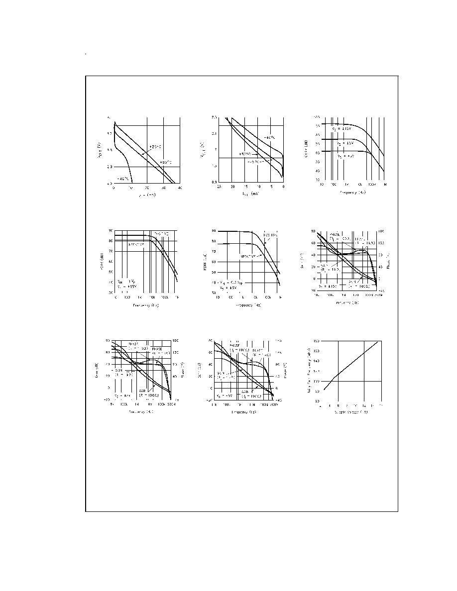
Supply Current vs
Supply Voltage
DS012348-66
Supply Current vs
Temperature
DS012348-67
Input Offset Voltage
vs Temperature
DS012348-68
www.national.com
6

Typical Performance Characteristics
T
A
= 25∞C, R
L
= 1 M
. unless otherwise specified (Continued)
Input Bias Current
vs Temperature
DS012348-69
Input Offset Voltage vs
Common Mode Voltage
@
V
S
=
±
15V
DS012348-76
Input Offset Voltage vs
Common Mode Voltage
@
V
S
=
±
5V
DS012348-77
Short Circuit Current
vs Temperature (Sourcing)
DS012348-78
Short Circuit Current
vs Temperature (Sinking)
DS012348-79
Output Voltage vs Output
Current (I
SINK
, V
S
=
±
15V)
DS012348-70
Output Voltage vs Output
Current (I
SOURCE
, V
S
=
±
15V)
DS012348-71
Output Voltage vs Output
Current (I
SOURCE
, V
S
=
±
5V)
DS012348-72
Output Voltage vs Output
Current (I
SINK
, V
S
=
±
5V)
DS012348-73
www.national.com
7

Typical Performance Characteristics
T
A
= 25∞C, R
L
= 1 M
. unless otherwise specified (Continued)
Output Voltage vs Output
Current (I
SOURCE
, V
S
= +5V)
DS012348-74
Output Voltage vs Output
Current (I
SINK
, V
S
= +5V)
DS012348-75
CMRR vs Frequency
DS012348-3
PSRR vs Frequency
DS012348-4
PSRR vs Frequency
DS012348-5
Open Loop Frequency
Response
DS012348-88
Open Loop Frequency
Response
DS012348-89
Open Loop Frequency
Response
DS012348-90
Unity Gain Frequency vs
Supply Voltage
DS012348-24
www.national.com
8

Typical Performance Characteristics
T
A
= 25∞C, R
L
= 1 M
. unless otherwise specified (Continued)
GBWP
@
10 MHz
vs Supply Voltage
DS012348-25
Large Signal Voltage Gain
vs Load, V
S
=
±
15V
DS012348-96
Large Signal Voltage Gain
vs Load, V
S
=
±
5V
DS012348-97
Input Voltage
Noise vs Frequency
DS012348-27
Input Current
Noise vs Frequency
DS012348-28
Input Voltage
Noise vs Frequency
DS012348-29
Input Current
Noise vs Frequency
DS012348-30
Slew Rate vs Supply Voltage
DS012348-31
Slew Rate vs Input Voltage
DS012348-32
www.national.com
9

Typical Performance Characteristics
T
A
= 25∞C, R
L
= 1 M
. unless otherwise specified (Continued)
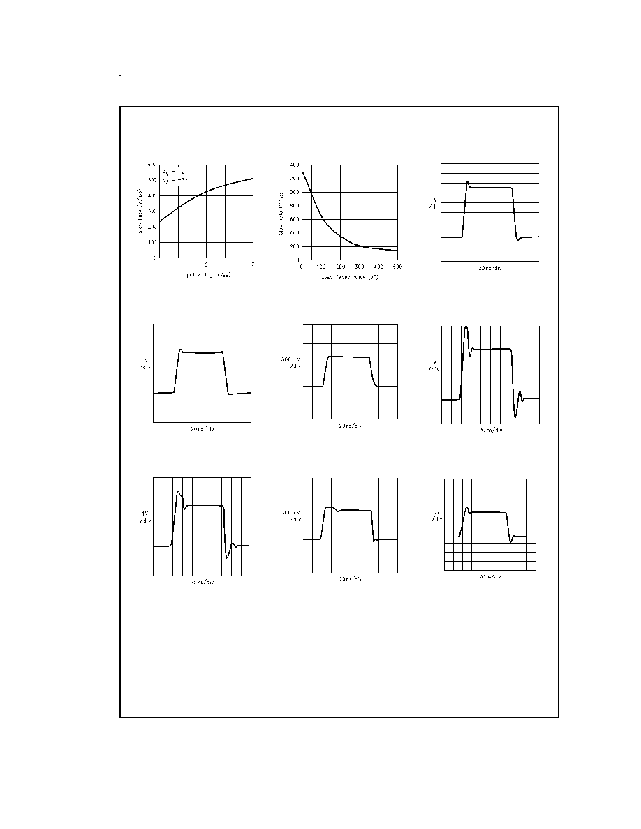
Slew Rate vs Input Voltage
DS012348-33
Slew Rate vs
Load Capacitance
DS012348-34
Large Signal Pulse Response,
A
V
= -1, V
S
=
±
15V
DS012348-35
Large Signal Pulse Response,
A
V
= -1, V
S
=
±
5V
DS012348-36
Large Signal Pulse Response,
A
V
= -1, V
S
= +5V
DS012348-37
Large Signal Pulse Response,
A
V
= +1, V
S
=
±
15V
DS012348-38
Large Signal Pulse Response,
A
V
= +1, V
S
=
±
5V
DS012348-39
Large Signal Pulse Response,
A
V
= +1, V
S
= +5V
DS012348-40
Large Signal Pulse Response,
A
V
= +2, V
S
=
±
15V
DS012348-41
www.national.com
10

Typical Performance Characteristics
T
A
= 25∞C, R
L
= 1 M
. unless otherwise specified (Continued)
Large Signal Pulse Response,
A
V
= +2, V
S
=
±
5V
DS012348-42
Large Signal Pulse Response,
A
V
= +2, V
S
= +5V
DS012348-43
Small Signal Pulse Response,
A
V
= -1, V
S
=
±
15V, R
L
= 100
DS012348-44
Small Signal Pulse Response,
A
V
= -1, V
S
=
±
5V,
R
L
= 100
DS012348-45
Small Signal Pulse Response,
A
V
= -1, V
S
= +5V,
R
L
= 100
DS012348-46
Small Signal Pulse Response,
A
V
= +1, V
S
=
±
15V,
R
L
= 100
DS012348-47
Small Signal Pulse Response,
A
V
= +1, V
S
=
±
5V,
R
L
= 100
DS012348-48
Small Signal Pulse Response,
A
V
= +1, V
S
= +5V,
R
L
= 100
DS012348-49
Small Signal Pulse Response,
A
V
= +2, V
S
=
±
15V,
R
L
= 100
DS012348-50
www.national.com
11

Typical Performance Characteristics
T
A
= 25∞C, R
L
= 1 M
. unless otherwise specified (Continued)
Small Signal Pulse Response,
A
V
= +2, V
S
=
±
5V,
R
L
= 100
DS012348-51
Small Signal Pulse Response,
A
V
= +2, V
S
= +5V,
R
L
= 100
DS012348-52
Closed Loop Frequency
Response vs Temperature
V
S
=
±
15V, A
V
= +1, R
L
= 100
DS012348-53
Closed Loop Frequency
Response vs Temperature
V
S
=
±
5V, A
V
= +1, R
L
= 100
DS012348-54
Closed Loop Frequency
Response vs Temperature
V
S
= +5V, A
V
= +1, R
L
= 100
DS012348-55
Closed Loop Frequency
Response vs Temperature
V
S
=
±
15V, A
V
= +2, R
L
= 100
DS012348-58
Closed Loop Frequency
Response vs Temperature
V
S
=
±
5V, A
V
= +2, R
L
= 100
DS012348-59
Closed Loop Frequency
Response vs Temperature
V
S
= +5V, A
V
= +2, R
L
= 100
DS012348-60
Closed Loop Frequency
Response vs Capacitive
Load (A
V
= +1, V
S
=
±
15V)
DS012348-61
www.national.com
12

Typical Performance Characteristics
T
A
= 25∞C, R
L
= 1 M
. unless otherwise specified (Continued)
Closed Loop Frequency
Response vs Capacitive
Load (A
V
= +1, V
S
=
±
5V)
DS012348-62
Closed Loop Frequency
Response vs Capacitive
Load (A
V
= +2, V
S
=
±
15V)
DS012348-63
Closed Loop Frequency
Response vs Capacitive
Load (A
V
= +2, V
S
=
±
5V)
DS012348-64
Total Harmonic Distortion
vs Frequency
DS012348-80
Total Harmonic Distortion
vs Frequency
DS012348-81
Total Harmonic Distortion
vs Frequency
DS012348-83
Total Harmonic Distortion
vs Frequency
DS012348-82
Undistorted Output Swing
vs Frequency
DS012348-85
Undistorted Output Swing
vs Frequency
DS012348-84
www.national.com
13

Typical Performance Characteristics
T
A
= 25∞C, R
L
= 1 M
. unless otherwise specified (Continued)
Application Information
The table below, depicts the maximum operating supply volt-
age for each package type:
TABLE 1. Maximum Supply Voltage Values
SOT23-5
SO-8
Single Supply
10V
30V
Dual Supplies
±
5V
±
15V
Stable unity gain operation is possible with supply voltage of
5V for all capacitive loads. This allows the possibility of using
the device in portable applications with low supply voltages
with minimum components around it.
Above a supply voltage of 6V (
±
3V Dual supplies), an addi-
tional resistor and capacitor (shown below) should be placed
in the feedback path to achieve stability at unity gain over the
full temperature range.
The package power dissipation should be taken into account
when operating at high ambient temperatures and/or high
power dissipative conditions. Refer to the power derating
curves in the data sheet for each type of package.
In determining maximum operable temperature of the de-
vice, make sure the total power dissipation of the device is
considered; this includes the power dissipated in the device
with a load connected to the output as well as the nominal
dissipation of the op amp.
The device is capable of tolerating momentary short circits
from its output to ground but prolonged operation in this
mode will damage the device, if the maximum allowed junc-
tion temperation is exceeded.
APPLICATION CIRCUITS
Current Boost Circuit
The circuit in
Figure 2 can be used to achieve good linearity
along with high output current capability.
By proper choice of R
3
, the LM7121 output can be set to
supply a minimal amount of current, thereby improving its
output linearity.
R
3
can be adjusted to allow for different loads:
R
3
= 0.1 R
L
The circuit above has been set for a load of 100
.
Reasonable speeds (
<
30 ns rise and fall times) can be ex-
pected up to 120 mA
PP
of load current (see
Figure 3 for step
response across the load).
Undistorted Output Swing
vs Frequency
DS012348-86
Total Power Dissipation
vs Ambient Temperature
DS012348-65
DS012348-87
FIGURE 1. Typical Circuit for A
V
= +1
Operation (V
S
6V)
DS012348-92
FIGURE 2. Simple Circuit to Improve Linearity
and Output Drive Current
www.national.com
14

Application Information
(Continued)
It is very important to keep the lead lengths to a minimum
and to provide a low impedance current path by using a
ground-plane on the board.
Caution: If R
L
is removed, the current balance at the output
of LM7121 would be disturbed and it would have to supply
the full amount of load current. This might damage the part if
power dissipation limit is exceeded.
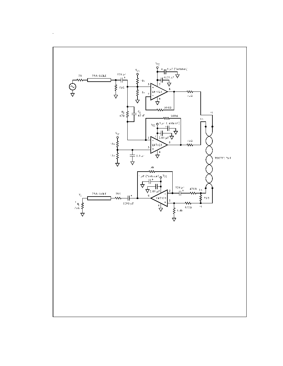
Color Video on Twisted Pairs Using Single Supply
The circuit shown in
Figure 4 can be used to drive in excess
of 25 meters length of twisted pair cable with no loss of reso-
lution or picture definition when driving a NTSC monitor at
the load end.
DS012348-93
FIGURE 3. Waveform across a 100
Load
www.national.com
15

Application Information
(Continued)
Differential Gain and Differential Phase errors measured at
the load are less than 1% and 1∞ respectively.
R
G
and C
C
can be adjusted for various cable lengths to com-
pensate for the line losses and for proper response at the
output. Values shown correspond to a twisted pair cable
length of 25 meters with about 3 turns/inch (see
Figure 5 for
step response).
The supply voltage can vary from 8.5V up to 30V with the
output rise and fall times under 12 ns. With the component
values shown, the overall gain from the input to the output is
about 1.
Even though the transmission line is not terminated in its
nominal characteristic impedance of about 600
, the result-
ing reflection at the load is only about 5% of the total signal
and in most cases can be neglected. Using 75
termination
instead, has the advantage of operating at a low impedance
and results in a higher realizable bandwidth and signal
fidelity.
DS012348-94
Note:
Pin numbers shown are for SO-8 package.
*
Input termination of NTSC monitor.
FIGURE 4. Single Supply Differential Twister Pair Cable Transmitter/Receiver
8.5V
V
CC
30V
www.national.com
16

Application Information
(Continued)
DS012348-95
FIGURE 5. Step Response to a 1 V
PP
Input Signal Measured across the 75
Load
DS012348-98
(a) A
V
= -1
DS012348-99
C
C
= 2 pF for R
L
= 100
C
C
= Open for R
L
= Open
(b) A
V
= +2
DS012348-A0
(c) A
V
= +2, Capacitive Load
DS012348-A1
R
F
= 0
, C
C
= Open for V
S
<
6V
R
F
= 510
, C
C
= 3 pF for V
S
6V
(d) A
V
= +1
DS012348-A2
(e) A
V
= +1, V
S
= +5V, Single Supply Operation
FIGURE 6. Application Test Circuits
www.national.com
17

Physical Dimensions
inches (millimeters) unless otherwise noted
8-Lead (0.150" Wide) Small Outline Package, JEDEC
Order Number LM7121IM or LM7121IMX
NS Package Number M08A
www.national.com
18

Physical Dimensions
inches (millimeters) unless otherwise noted (Continued)
LIFE SUPPORT POLICY
NATIONAL'S PRODUCTS ARE NOT AUTHORIZED FOR USE AS CRITICAL COMPONENTS IN LIFE SUPPORT
DEVICES OR SYSTEMS WITHOUT THE EXPRESS WRITTEN APPROVAL OF THE PRESIDENT AND GENERAL
COUNSEL OF NATIONAL SEMICONDUCTOR CORPORATION. As used herein:
1. Life support devices or systems are devices or
systems which, (a) are intended for surgical implant
into the body, or (b) support or sustain life, and
whose failure to perform when properly used in
accordance with instructions for use provided in the
labeling, can be reasonably expected to result in a
significant injury to the user.
2. A critical component is any component of a life
support device or system whose failure to perform
can be reasonably expected to cause the failure of
the life support device or system, or to affect its
safety or effectiveness.
National Semiconductor
Corporation
Americas
Tel: 1-800-272-9959
Fax: 1-800-737-7018
Email: support@nsc.com
National Semiconductor
Europe
Fax: +49 (0) 1 80-530 85 86
Email: europe.support@nsc.com
Deutsch Tel: +49 (0) 1 80-530 85 85
English
Tel: +49 (0) 1 80-532 78 32
FranÁais Tel: +49 (0) 1 80-532 93 58
Italiano
Tel: +49 (0) 1 80-534 16 80
National Semiconductor
Asia Pacific Customer
Response Group
Tel: 65-2544466
Fax: 65-2504466
Email: sea.support@nsc.com
National Semiconductor
Japan Ltd.
Tel: 81-3-5639-7560
Fax: 81-3-5639-7507
www.national.com
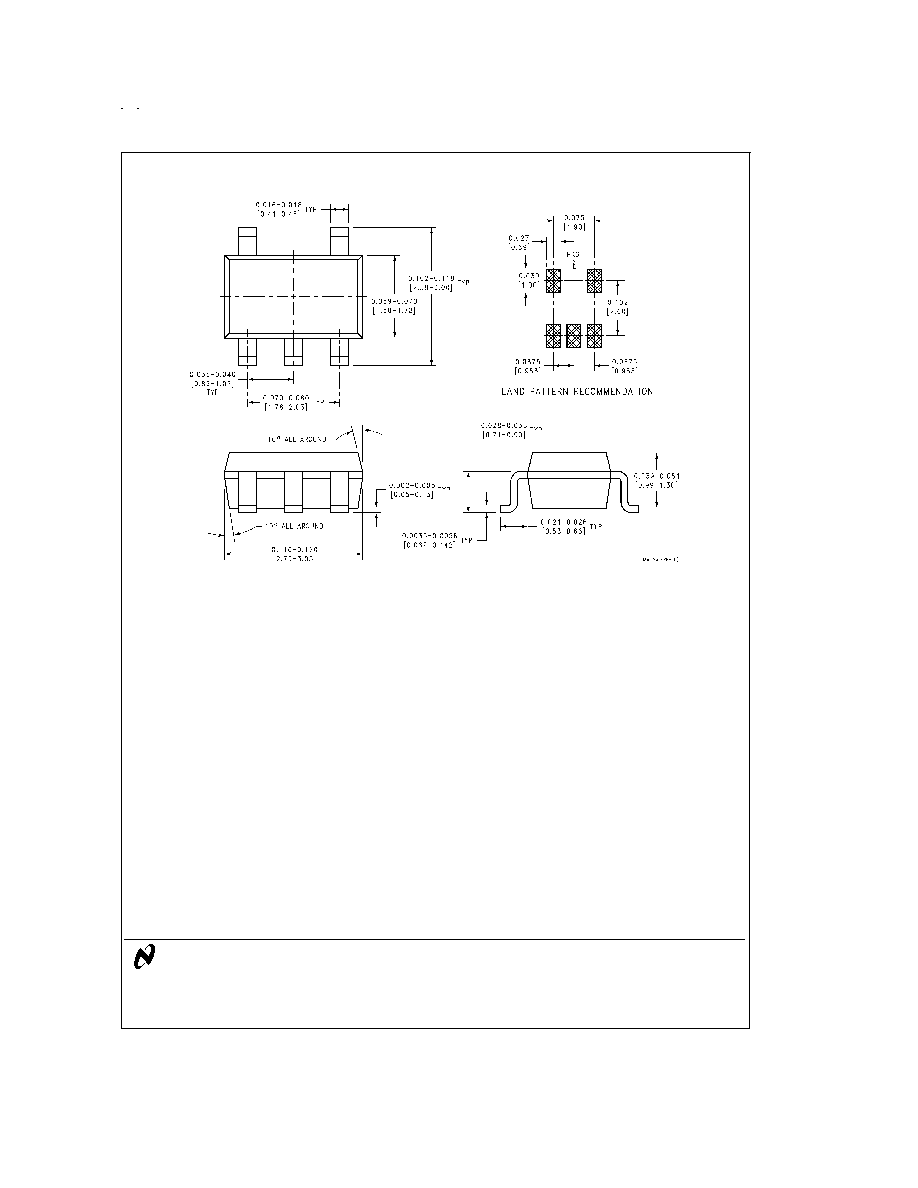
5-Lead Molded SOT23-5
Order Number LM7121IM5 or LM7121IM5X
NS Package Number MA05A
LM7121
235
MHz
T
iny
Low
Power
V
oltage
Feedback
Amplifier
National does not assume any responsibility for use of any circuitry described, no circuit patent licenses are implied and National reserves the right at any time without notice to change said circuitry and specifications.


